A Unified Charge-current VS Compact Model for Graphene Transistors Applicable in Analog Circuit Simulations
- Category: Circuits & Systems, Electronic Devices
- Tags: dimitri antoniadis, shaloo rakheja
With its rich physics, graphene has properties that make it a viable candidate for implementing electronic devices. For example, graphene as a two-dimensional material has a limited phase space for scattering of electrons; hence, the electrons in graphene can have a long MFP–a property that can be utilized to build high frequency devices[1],[2]. However, to design and simulate electronic circuits built with graphene transistors, compact device models are needed to describe electron transport in both long and short-channel graphene field effect transistors (GFETs).
In this work, we extend the compact virtual source (VS) model originally developed for silicon transistors[3] to describe current conduction in quasi-ballistic graphene transistors. Because of the absence of bandgap in graphene, graphene can uniquely exhibit ambipolar transport[4]. Hence, the VS model is adjusted from the original VS model for silicon to accurately describe current conduction in ambipolar regime in GFETs (see Figures 1b and 1b). The key parameters of the VS model- apparent channel mobility, µapp, and the virtual source velocity, vxo, are extracted from published experimental results on short-channel GFETs[5]. It is found that vxo in quasi-ballistic GFETs can be quite large compared to its value for silicon FETs with similar channel lengths. This velocity is attributed to the large effective mobility, µeff, in graphene for technologically relevant carrier concentrations (see Figure 2)[6].
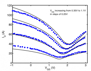
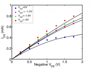
The physics of electron transport in long-channel GFETs can be described fairly accurately within the drift diffusion (DD) transport framework. The DD-model for GFETs is used to explain the experimental findings in[7],[8], and reasonable match with experimental data is demonstrated (see Figures 3a and 3b). Both VS and DD current models are implemented in Verilog-A to provide a platform for simulation of basic analog circuits such as frequency multipliers with graphene.
Future work includes introducing intrinsic charge partitioning, and therefore an intrinsic capacitance model, that will be strictly consistent with both the quasi-ballistic VS model in both nano-scale unipolar and ambipolar GFETs and the DD model for long-channel unipolar and ambipolar GFETs.
-
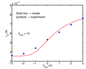
- Figure 1a: ID versus VGS of the top gate in graphene for a VDS of 1V. Experimental data from [5] for a channel length is 240 nm and channel width of 1 µm. The extracted mobility is 1480 cm2/Vs and vxo = 2.5e7 cm/s.
-
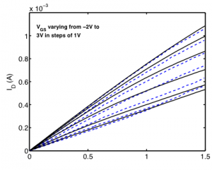
- Figure 1b: Output curves for the device shown in Figure 1a. Dotted lines correspond to experimental data, while solid lines correspond to the VS model.
-
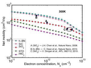
- Figure 2: Effective mobility versus carrier concentration in graphene on various substrates at room temperature. Graphene on h-BN offers the best-case effective mobility because it is lattice matched with graphene and has a weaker Fröhlich coupling of surface polar phonons with graphene sheet[9].
-
- Figure 3a: Experimental data (symbols) for the device of length and width = 5 µm from[10]. The drift-diffusion model is fitted as shown in solid lines.
-
- Figure 3b: Output characteristics for experimental data (symbols) [8] for the device of length = 1 µm and width = 2.1 µm from[11]. The drift-diffusion model is fitted as shown in solid lines.
- A. H. Castro Neto, F. Guinea, K. S. Novoselov, and A. K. Geim, “The electronic properties of graphene,” Review of Modern Physics, vol. 81, no. 1, pp. 109-162, Jan.-Mar. 2009. [↩]
- H. Wang, A. Hsu, J. Wu, J. Kong, T. Palacios, “Graphene-based ambipolar RF-mixers,” IEEE Electron Device Letters, vol. 31, no. 9, pp. 906-908, 2010. [↩]
- A. Khakifirooz, O.M. Nayfeh, and D. Antoniadis, “A simple semi-empirical semi-empirical short-channel MOSFET current-voltage model continuous across all regions of operation and employing only physical parameters,” IEEE Transactions on Electron Devices, vol. 56, no. 8, pp. 1674-1680, Aug. 2009. [↩]
- T. Palacios, A. Hsu, and H. Wang, “Applications of graphene devices in RF communications,” IEEE Communications Magazine, vol. 48, no. 6, pp. 122-128, June 2010. [↩]
- Y. Lin, C. Dimitrakopoulos, K.A. Jenkins, D.B. Farmer, H.-Y. Chiu, A. Grill, and P.H. Avouris, “100-GHz transistors from wafer-scale epitaxial graphene,” Science, vol. 327, no. 5966, p. 663, Feb. 2010. [↩]
- S. Rakheja, V. Kumar, A. Naeemi, “Evaluation of the potential performance of graphene nanoribbons as on-chip interconnects (invited),” Proceedings of the IEEE, vol. 101, no.7, 2013. [↩]
- H. Wang, A. Hsu, J. Kong, D. A. Antoniadis, and T. Palacios, “Compact virtual-source current-voltage model for top- and back-gated graphene field-effect transistors,” IEEE Transactions on Electron Devices, vol. 58, no. 5, May 2011. [↩]
- I. Meric, M.Y. Han, A. F. Young, B. Ozyilmaz, P. Kim, and K. A. Shepard, “Current saturation in zero-bandgap graphene field-effect transistors,” Nature Nanotechnology, vol. 3, pp. 654-659, Nov. 2008. [↩]
- S. Rakheja, V. Kumar, A. Naeemi, “Evaluation of the potential performance of graphene nanoribbons as on-chip interconnects (invited),” Proceedings of the IEEE, vol. 101, no.7, 2013. [↩]
- H. Wang, A. Hsu, J. Kong, D. A. Antoniadis, and T. Palacios, “Compact virtual-source current-voltage model for top- and back-gated graphene field-effect transistors,” IEEE Transactions on Electron Devices, vol. 58, no. 5, May 2011. [↩]
- Y. Lin, C. Dimitrakopoulos, K.A. Jenkins, D.B. Farmer, H.-Y. Chiu, A. Grill, and P.H. Avouris, “100-GHz transistors from wafer-scale epitaxial graphene,” Science, vol. 327, no. 5966, p. 663, Feb. 2010. [↩]