Nano-scale Metal Contacts for III-V FETs
- Category: Electronic Devices, Nanotechnology
- Tags: III-V materials, jesus del alamo, wenjie lu
In the last few years, III-V compound semiconductors have emerged as a promising family of materials to replace silicon in logic applications[1]. Novel III-V MOSFET prototypes with superior electron-transport properties have been recently demonstrated[2]. One of the challenges to obtain high performance is to achieve a very low ohmic contact resistance. As transistor scaling continues, it is important to fabricate and characterize high-quality ohmic contacts with nanometer-scale contact length. In this project, a nano-scale transmission line model (nano-TLM) structure is being developed to study and optimize metal contacts for III-V field-effect transistors.
This works builds on prior research in our group on the fabrication and characterization of nanoscale contacts to III-V FET structures[3]. Our nano-TLM structure comprises a Mo contact on an InGaAs heterostructure, with various contact lengths (Lc) and spacings (Ld). The Mo contact is patterned by electron beam lithography, followed by reactive-ion etching (RIE). The mesa isolation and contact pads are fabricated by a series of lithography, RIE, and lift-off processes. The ohmic contact is annealed at 400 °C for 40 s. Figure 1 shows a nano-TLM with Lc = 19 nm, the smallest contacts we have fabricated at present. The finished test structures are characterized using Kelvin 4-terminal measurement. We developed a 2-D circuit model to extract the contact resistivity, semiconductor sheet resistance, and metal sheet resistance. Figure 2 shows resistance measurements on Mo-n+-InGaAs structures with 80-nm contact length and various contact spacings. From measurements of this kind in several structures, an average contact resistivity of 0.6 Ω∙μm2 is obtained.
Our research will continue to optimize the contact fabrication to achieve lower contact resistance and further scaling. We will also investigate the contact resistance to a buried channel. We will further explore metals contacts on p-type Sb-based heterostructures, which are as critical as the n-type counterpart but in great need of a high-quality ohmic contact.
-
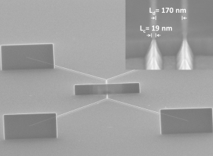
- Figure 1: SEM image showing the top view of a Mo-n+-InGaAs nano-TLM structure, with contact length Lc = 19 nm. The inset is a close view of Mo contacts at the edge of the mesa.
-
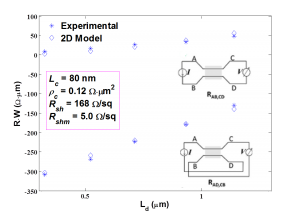
- Figure 2: Experimental nano-TLM resistance of test structures with average contact length of 80 nm. The values of ρc, Rsh, and Rshm are extracted by the 2D nano-TLM model. The insets show the two configurations in the Kelvin measurements.
- J. A. del Alamo, “Nanometre-scale electronics with III-V compound semiconductors,” Nature, vol. 479, no. 7373, pp. 317-323, Nov. 2011. [↩]
- J. Lin, D. A. Antoniadis, and J. A. del Alamo, “Sub-30 nm InAs quantum-well MOSFETs with self-aligned metal contacts and sub-1 nm EOT HfO2 insulator.” IEEE International Electron Devices Meeting, San Francisco, CA, December 10-12, 2012, pp. 757-760. [↩]
- A. Guo and J. A. del Alamo, “Mo/n+-InGaAs nanocontacts for future III-V MOSFETs,” 25th International Conference on Indium Phosphide and Related Materials, Kobe, Japan, May 19-23, 2013. [↩]