Fabrication Technology for InGaAs/GaAsSb Vertical Tunnel-FETs
- Category: Electronic Devices
- Tags: judy l hoyt, tao yu
With the continuing downscaling of the modern complementary metal–oxide–semiconductor (CMOS) technology, integrated circuit power consumption has become one of the most critical issues. This development is due to the limit of operation voltage scaling, which originates from the limit of 60mV/dec sub-threshold swing in the conventional MOS devices[1]. Various device structures have been proposed to achieve sub-threshold swing below 60mV/dec using novel device physics, including impact ionization[2], interband tunneling[3], etc. In particular, tunnel-field-electron transistors (T-FETs) have attracted much attention due to their potential of achieving sharp subthreshold behavior, CMOS compatibility, and scalability[4]. Vertical T-FETs with a heterojunction structure have been proposed to yield higher tunneling efficiency, and thus larger tunneling current[4], and are potential candidates for future-generation low-power technology. In this study, InGaAs/GaAsSb heterojunction vertical T-FETs were designed and fabricated to investigate the impacts of different structural parameters.
The cross-sectional view of the InGaAs/GaAsSb vertical T-FET appears in Figure 1. The tunneling path from p+-GaAsSb to n-InGaAs is highlighted. To ensure complete gate control over the region where tunneling takes place, an air-bridge structure is implemented, eliminating potential leakage paths due to tunneling without gate-control. Figure 2 shows the proposed process flow. The molybdenum drain contact is deposited and patterned first, followed by mesa definition and etch. Then a HfO2 gate dielectric and a tungsten gate are deposited after surface passivation. The air-bridge structure is formed by dry etching fins followed by a selective wet etch that undercuts the fin and suspends the air-bridges. Figure 2a shows an SEM micrograph of the air-bridge structure after lateral undercut etch. After the air-bridge formation, etching the n-InGaAs in the source region exposes the source. Then the Pd/Au contact is deposited on the p+-GaAsSb layer. The inter-layer dielectric is then deposited, via holes are opened for contact, and finally, probe pads are formed. The impacts of different structural parameters on device performance are under study.
-
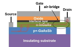
- Figure 1: Cross-sectional view of the InGaAs/GaAsSb vertical T-FET. An air-bridge structure is implemented to eliminate potential leakage paths.
-
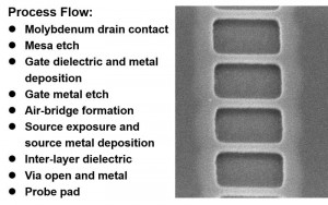
- Figure 2: Left: Proposed process flow for the InGaAs/GaAsSb vertical T-FET. Right: SEM micrograph of the fabricated air-bridge structure after a selective wet etch.
- T. Yuan and T. H. Ning, Fundamentals of Modern VLSI Devices, 2nd Edition, Cambridge: Cambridge University Press, 2004. [↩]
- K. Gopalakrishnan, P. B. Griffin, and J. D. Plummer, “Impact ionization MOS (I-MOS)-Part I: device and circuit simulations,” IEEE Trans. Electron Devices, vol. 52, no. 1, pp. 69-76, 2005 [↩]
- J. Appenzeller, Y.-M. Lin, J. Knoch, and P. Avouris, “Band-to-Band Tunneling in Carbon Nanotube Field-Effect Transistors,” Phys. Rev. Lett., vol. 93, p. 196805, 2004. [↩]
- A. M. Ionescu and H. Riel, “Tunnel field-effect transistors as energy-efficient electronic switches,” Nature, vol. 479, no. 7373, pp. 329–337, 2011. [↩] [↩]