High Linearity GaN HEMTs with Nanowire Channel
- Category: Electronic Devices
- Tags: dong seup lee, tomas palacios
The performance of GaN-based high-electron-mobility transistors (HEMTs) has been significantly improved over the last two decades through extensive research[1][2][3]. However, the demonstrated device characteristics are still below theoretical expectations based on GaN material properties, and several unsolved problems remain for large-signal RF operation of these devices. One of the critical issues is the non-linear behavior of short-channel GaN HEMTs. In conventional GaN devices, the extrinsic transconductance (gm) drops quickly with increasing drain current after reaching its peak value, and this issue becomes more serious as the gate length scales down. Another important issue is that a maximum drain current density in conventional short-channel GaN devices is still far below the theoretical value given by q·ns·vsat, where q is electron charge, ns is electron sheet charge density, and vsat is saturation velocity.
To address these two issues, we have demonstrated a HEMT with a nanowire channel structure as shown in Figure 1. We found that the increase of source access resistance with drain current severely limits the linearity of GaN HEMTs. When the ratio of the source access region width to that of the channel increases, the transistor access region has a larger current drivability than the channel region, which enables the source access region to behave more like an ideal source. The suppression of the increase in source access resistance with current provides a flat transconductance (gm) at high drain current even in sub-100-nm short-channel devices as shown in Figure 2. Moreover, the constant source resistance allows a higher effective gate voltage overdrive, which enables a higher drain current density (over 3.5 A/mm) in the intrinsic device. The new devices also show very flat current-gain cut-off frequency (fT) as a function of gate voltage. These results highlight the importance of the source access region in limiting the maximum current density and the linearity of GaN HEMTs.
-
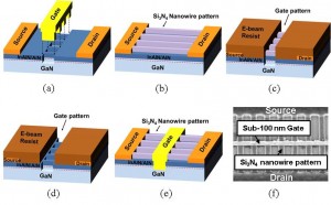
- Figure 1: Device structure of nanowire channel HEMT and its fabrication process.
-
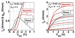
- Figure 2: Comparison of DC (a) transfer and (b) output characteristics of Lg=70-80-nm nanowire channel device with planar device.
- K. Shinohara, D. Regan, A. Corrion, D. Brown, Y. Tang, J. Wong, G. Candia, A. Schmitz, H. Fung, S. Kim and M. Micovic, “Self-Aligned-Gate GaN HEMTs with Heavily-Doped n+-GaN Ohmic Contacts to 2DEG, ” IEDM Tech. Dig., 2012, paper 27.2, pp. 617-620. [↩]
- Y. Yue, Z. Hu, J. Guo, B. Sensale-Rodriguez, G. Li, R. Wang, f. Faria, T. Fang, B. Song, X. Gao, S. Guo, T. Kosel, G. Snider, P. Fay, D. Jena, H. Xing, “InAlN/GaN HEMTs with Regorwn Ohmic Contacts and fT of 370 GHz,” IEEE Electron Dev. Lett., vol. 33, no. 7, pp. 988-990, July 2012. [↩]
- D. S. Lee, X. Gao, S. Guo, D. Kopp, P. Fay, T. Palacios, “300-GHz InAlN/GaN HEMTs with InGaN Back-Barrier,” IEEE Electron Dev. Lett., vol. 32, no. 11, pp. 1525-1527, Nov. 2011. [↩]