Next-Generation Ultrafast Photo-Triggered Cathodes
- Category: Electronic Devices, Nanotechnology, Optics & Photonics
- Tags: luis velasquez-garcia, michael swanwick
State-of-the-art ultrafast cathodes are based on the photoelectric effect, where electrons are emitted from a flat surface using ultraviolet (UV) pulses; however, these cathodes have a number of shortcomings including difficult manufacture, need for ultra-high vacuum to operate, and short lifetime[1]. Photon-triggered field emission cathodes are an attractive alternative to circumvent these issues. Strong-field electron tunneling from solids without damage occurs when the electric field of high-intensity optical pulses interacts with field enhancing structures to lower the incident flux necessary for barrier suppression. In this project we are using wafer-level semiconductor batch fabrication techniques to create massively multiplexed arrays of nano-sharp high-aspect-ratio silicon pillars with high uniformity (4.6-million tips.cm-2), resulting in greatly enhanced array electron emission. A high-aspect-ratio silicon column topped by a nano-sharp tip achieves electron emission at low power by greatly enhancing the incident electric field, and the massive multiplexing of the pillars drastically increases the total current emission. We developed a fabrication process that attains small tip variation across the array due to the diffusion-limited oxidation step that sharpens the tips, resulting in large array utilization. As shown in Fig. 1, the high field of the ultra-short laser pulses combined with the field enhancement of the nano-sharp high-aspect-ratio silicon tip array resulted in large current emission using small laser energies. Between 25 nJ and 0.1 µJ laser pulse energy, the data follow a multi-photon absorption process; the high power dependence of the emitted current on the laser pulse energy comes from the electrons oscillating back into the tip. For larger laser pulse energies the curve bends over, evidencing operation of the cathode in the tunneling regime[2]; this transition occurs because the electric field becomes so strong that the electrons tunnel faster than they can oscillate back into the tips. We have also demonstrated long-term operation without degradation for 3.6 nA average current from an array of about 2,220 tips[3].
-
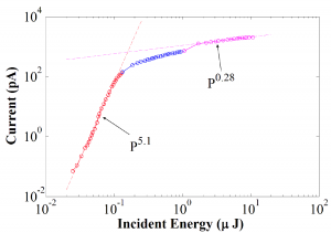
- Log-log plot of emitted current versus incident laser pulse energy for 10 V anode voltage[4]
-
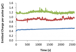
- Photo-emitted current versus time. Top green line is 9.5 µJ with 1000 V anode bias, middle red line is 9.5 µJ with 500 V anode bias and the bottom blue line is 3.0 µJ with 500 V anode bias[5]
- Q. Guo, K. Takahashi, K. Saito, H. Akiyama, T. Tanaka, and M. Nishio, “Band alignment of ZnTe/GaAs heterointerface investigated by synchrotron radiation photoemission spectroscopy,” Applied Physics Letters, vol. 102, no. 9, pp. 092107–092107–4, Mar. 2013. [↩]
- M. Swanwick, P. D. Keathley, F. X. Kärtner, and L. F. Velásquez-García, “Ultrafast Photo-Triggered Field Emission Cathodes Using Massive, Uniform Arrays Of Nano-Sharp High-Aspect-Ratio Silicon Structures”, Technical Digest of the 17th International Conference on Solid-State Sensors, Actuators, and Microsystems, Barcelona, Spain, pp. 2680 – 2683, June 16 – 20 2013. [↩]
- M. Swanwick, P. D. Keathley, F. X. Kärtner, and L. F. Velásquez-García, “Nanostructured Silicon Photo-cathodes for X-ray Generation”, Technical Digest of the 26th International Vacuum Nanoelectronics Conference, Roanoke VA, July 8 – 12 2013. [↩]
- [M. Swanwick, P. D. Keathley, F. X. Kärtner, and L. F. Velásquez-García, “Ultrafast Photo-Triggered Field Emission Cathodes Using Massive, Uniform Arrays Of Nano-Sharp High-Aspect-Ratio Silicon Structures”, Technical Digest of the 17th International Conference on Solid-State Sensors, Actuators, and Microsystems, Barcelona, Spain, pp. 2680 – 2683, June 16 – 20 2013. [↩]
- M. Swanwick, P. D. Keathley, F. X. Kärtner, and L. F. Velásquez-García, “Nanostructured Silicon Photo-cathodes for X-ray Generation”, Technical Digest of the 26th International Vacuum Nanoelectronics Conference, Roanoke VA, July 8 – 12 2013. [↩]