TEM Studies of Degradation Studies of AlGaN High Electron Mobility Transistors
- Category: Electronic Devices
- Tags: carl thompson, swee ching tan
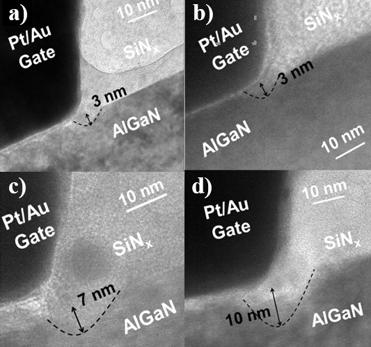
Figure 1: Cross sectional TEM images at the drain edge of the gate in the AlGaN/GaN HEMTs stressed at Vgs = -7 V and Vds = 43 V for 3000s in vacuum of 1×10⁻⁷ Torr (a) dry air (b) ambient air (c) and in water saturated air (d).
AlGaN/GaN High Electron Mobility Transistors (HEMT) are candidate for high-power amplifiers. However, for wide scale implementation reliability issues for these devices must be overcome. AlGaN/GaN devices have typically shown rapid degradation in output power and drain current within a short time during high voltage off-state stress. The degradation mechanisms studied to date for these devices are related to the formation of physical defects (pits and cracks) in the drain-side of the gate under high-voltage off-state stress[1][2]. It has been proposed that a field-induced inverse piezoelectric effect of AlGaN material might play a role in causing surface cracking and pitting[2][3]. On the other hand, it has also been proposed that the pits could be caused by electrochemical reactions at the surface due to the combination of high electric field and oxygen[4][5]. However, direct experimental evidence and detailed mechanisms for the nature of this structural degradation in AlGaN/GaN HEMTs is still needed.
A series of experiments was carried out in which devices were degraded in different ambients (water saturated air, ambient air, dry air and vacuum), in the off-state mode. We found that the size of the pits that formed was dependent on the amount of moisture present in the ambient. Cross sectional transmission electron microscopy (TEM) images of these devices at the drain edge of the gate after electrical stressing at Vgs = -7 V and Vds = 43 V for 3000s under the four different ambient conditions are shown in Figure 1. Pit formation is clearly seen to occur through a water-assisted reaction, most likely through electrochemical reactions at the gate edge.
- S.Y. Park, C. Floresca, U. Chowdhury, J. L. Jimenez, C. Lee, E. Beam, P. Saunier, T. Balistreri, and M.J. Kim, “Physical dedgradation of GaN HEMT devices under high drain bias reliability testing,” Microelectron Reliablity, vol. 49, no. 5, pp. 478-483, 2009. [↩]
- J. Joh, J.A. del Alamo, “Critical voltage for electrical degradation of GaN high-electron mobility transistors, “IEE Electron Dev. Letters, vol. 29, no. 4, pp. 287-289, 2008. [↩] [↩]
- J.A. del Alamo and J. Joh, “GaN HEMT reliability,” Microelectron Reliability, vol. 49, no. 5, pp. 1200-1206, 2009. [↩]
- P. Makaram, J. Joh, J.A. del Alamo, T. Palacios and C.V. Thompson, “Evolution of structural defects associated with electrical degradation in AlGaN/GaN high electron mobility transistors, “ Applied Physics Letters, vol. 96, no. 23, pp. 233509, 2010. [↩]
- F. Gao, B. Lu, L. Li, S. Kaun, J.S. Speck, C.V. Thompson and T. Palacios, “Role of Oxygen in the OFF-state degradation of AlGaN/GaN high electro mobility transistors,” Applied Physics Letters, vol. 99, no. 22, pp. 223506, 2011. [↩]