Quantization in Bilayer Tunneling Transistors
- Category: Electronic Devices, Nanotechnology
- Tags: dimitri antoniadis, james teherani
Tunneling field-effect transistors (TFETs)[1] are promising for low-power applications due to their potential to achieve a subthreshold swing (SS) lower than 60 mV/decade at room temperature. The bilayer TFET design is a novel double-gate structure that eliminates doping in the channel of the device and creates a hole-rich and electron-rich layer using oppositely biased top and bottom gates[2]. This gate-controlled electrostatic doping enables sharper p-n regions and a sharper density of states as there is no acceptor or donor impurity band. These benefits may allow for steeper switching of the bilayer TFET compared to conventional designs.
The structure and energy bands of a bilayer TFET are shown in Figure 1. The structure is similar to a thin-body double-gated device, except that the top and bottom gates are offset from each other. The structure is biased so as to create a hole-rich layer along the bottom gate connecting to the p+ source and an electron-rich layer along the top-gate connecting to the n+ drain. A small positive bias is applied to the drain, so that the whole structure is essentially a reverse-biased p-n junction. The small reverse-biased current is the off-state current of the device. The device can be turned on by applying a sufficient voltage across the top and bottom gates to make the electron and hole eigenstates overlap in energy. Once these states overlap, electrons can tunnel from the valence band into the conduction band. The sharpness of the transition from the off-state to the on-state depends on the sharpness of the density of states and can be degraded by parasitic tunneling through traps and other defects.
Since tunneling current is exponentially dependent on tunneling distance, on-current can be increased by decreasing the body thickness of the device. However, as the body thickness is made increasingly thin, the quantization energy of the electron and hole states becomes exceedingly large and requires a very large body voltage for the electron and hole eigenstates to overlap (Figure 2). In particular, the large body voltage is undesirable due to increased gate leakage. We have found that a 15-nm body thickness represents a reasonable tradeoff between on-state current and off-state gate leakage current in a bilayer TFET.
-
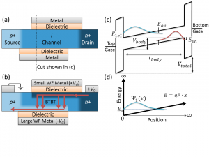
- Figure 1: (a) Electron-hole bilayer TFET structure. (b) Structure with bias and current flow. Red arrows indicate current path. A positively biased top gate attracts electrons while a negatively biased bottom gate attracts holes. Vertical band-to-band tunneling (BTBT) takes place when sufficient voltage is applied across the device so that the electron and hole eigenstates overlap in energy. (c) Energy band diagram across cut shown in (a). A triangular well forms near the top gate for electrons and near the bottom gate for holes. (d) Potential barrier problem solved analytically.
-
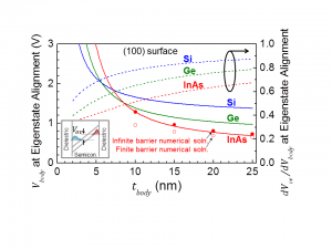
- Figure 2: Solid lines indicate the body voltage required to align the electron and hole eigenstates (required for the onset of band-to-band tunneling). A thin body thickness requires a large body voltage due to the increased confinement of electrons and holes. Dotted lines indicate the body-voltage efficiency—the change in the energy overlap of the electron and hole confined states for a change in the body voltage. The body-voltage efficiency is less than one because increasing the body voltage increases the confinement energy of electrons and holes.
- A. C. Seabaugh and Q. Zhang, “Low-Voltage Tunnel Transistors for Beyond CMOS Logic,” in Proceedings of the IEEE, vol. 98, no. 12, pp. 2095–2110, 2010. [↩]
- J. T. Teherani, S. Agarwal, E. Yablonovitch, J. L. Hoyt, and D. A. Antoniadis, “Impact of Quantization Energy and Gate Leakage in Bilayer Tunneling Transistors,” IEEE Electron Device Letters, vol. 34, no. 2, pp. 298 –300, Feb. 2013. [↩]