Degradation of GaN HEMTs under High-power and High-temperature Conditions
- Category: Electronic Devices
- Tags: jesus del alamo, yufei wu
Due to the wide band gap energy and high breakdown electric field of GaN, heterostructure transistors made from it are promising candidates for high power and high frequency applications. However, one issue that prevents the wide deployment of GaN HEMTs is their reliability. Research has been actively trying to improve the reliability of these devices. In spite of this, detailed understanding of the physics of device degradation mechanisms is still lacking[1]. Our research aims to fill this gap.
Previous studies have shown that under OFF-state stress, GaN HEMT degradation is dominated by a defect formation mechanism through the inverse piezoelectric effect [1]. This research studies GaN HEMT degradation under a more practical stress condition, i.e., the high power state. Devices were biased at VDS = 40V and IDQ = 100mA/mm, and the base temperature was stepped from 50°C to above 200°C. Experiments of this kind allow us to examine the role of temperature in high-power degradation in a single device. We have observed a degradation pattern for IGoff (defined @ VGS = -5V, VDS = 0.1V) that highly depends on stress temperature. Above a critical temperature, a sudden increase occurs (shown in Figure 1). We attribute this increase to physical defects formed along the gate edge at the drain side in the GaN cap layer. The degradation of IDmax (defined @ VDS = 5V, VGS = 2V), on the other hand, is more complex (Figure 2) and involves two different mechanisms, i.e., a trap-related degradation and a thermally activated permanent degradation. Also, IDmax degradation takes place only once IGoff degradation is saturated. We have been able to extract activation energies for both IDmax and RD degradation, and the two agree well. Our hypothesis for device degradation in the high-power state is that first the thin GaN cap layer is damaged, resulting in an increase in gate leakage current. Then the AlGaN barrier layer is exposed and starts getting damaged through the formation of pits. This damage leads to permanent drain current and drain resistance degradation. As the pits in the AlGaN barrier continue to grow in size, trapping effects related to such defects also increase. To verify our hypothesis, future studies will focus on the degradation behavior of devices with various cap layer thicknesses and Al compositions under the same stress conditions.
-
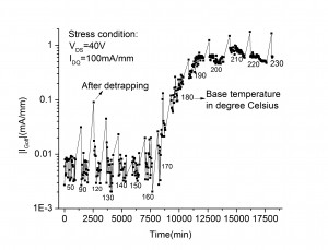
- Figure 1: Degradation of gate leakage current IGoff during high-power state stress in a step-temperature experiment from 50°C to 230°C and when the device characterization is conducted at 50°C. The numerical labels next to the data indicate the base plate temperature. A sudden increase in IGoff occurs at a base temperature stress of 170°C.
-
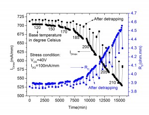
- Figure 2: Degradation of drain current and drain resistance in a step-temperature stress experiment under high-power bias. Both show thermally activated behavior. The extracted activation energies for permanent IDmax and RD degradations are 0.93 eV and 0.95 eV, respectively. The experiment setup differs from the one in Figure 1 in that two temperature ramps from 50°C to 220°C with a step of 20°C (not shown) were first carried out in order to bring IGoff degradation into saturation, and the device again was characterized at 50°C. Similar to the experiment in Figure 1, IDmax degradation occurs only after IGoff degradation is saturated.
- J. A. del Alamo and J. Joh, “GaN HEMT reliability,” Microelectronics Reliability, vol. 49, pp. 1200-1206, July 2009. [↩]