Device-level Thermal Analysis of GaN-based Electronics
- Category: Electronic Devices, Energy
- Tags: kevin bagnall, tomas palacios
Gallium nitride (GaN)-based electronics are one of the most exciting areas of innovation for high-frequency and high-voltage semiconductor devices. Although AlGaN/GaN power amplifiers (PAs) are capable of providing 40 W/mm RF output power[1], their performance has been severely limited by self-heating issues. In particular, intense Joule heating in the channel leads to high device temperatures and degraded performance and reliability. In this work, we are endeavoring to gain a fundamental understanding of thermal issues in GaN-based electronics in order to develop next-generation thermal management technologies to maximize the performance of GaN devices.
Despite the great amount of modeling and experimental investigations of thermal issues in GaN high electron mobility transistors (HEMTs), a number of important issues are poorly understood. For instance, the way to define the appropriate shape and length of the heat source in GaN HEMTs for thermal models is unclear. We have performed electro-thermal modeling in Silvaco ATLAS in order to quantitatively analyze the heat source distribution in AlGaN/GaN HEMTs under DC bias. As seen in Fig. 1, we have found that the heat source is highly non-uniform and extends over a region much larger than the gate length, in contrast to previous reports[2]. Although a conclusive study is forthcoming, our results also demonstrate that the heat source shape is strongly dependent on the DC bias condition and the gate-drain spacing.
We have also investigated a number of other important issues in thermal analysis of GaN HEMTs, including the importance of the substrate thermal boundary condition, temperature-dependent thermal conductivity, and temperature rise during switching transitions[3]. These investigations have led to the development of advanced analytical thermal models for GaN HEMTs[4] and a new extension to the Kirchhoff transform, a technique for solving heat conduction problems with temperature-dependent thermal conductivity[5]. As shown in Fig. 2, these analytical solutions are very accurate compared to full, non-linear numerical models and significantly reduce the computation time associated with evaluating the device temperature in multi-finger HEMTs.
-
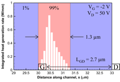
- Figure 1: Heat source distribution along the channel for AlGaN HEMT under DC bias (VG = -2 V, VD = 50 V, Ploss ~ 4 W/mm) obtained from Silvaco electro-thermal modeling.
-
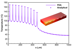
- Figure 2: Temperature distribution along the centerline of multi-finger GaN HEMT for RF power amplifier applications. Plot shows a comparison between a non-linear FEA model and an analytical model with the new Kirchhoff transform extension.
- Y.-F. Wu, M. Moore, A. Saxler, T. Wisleder, and P. Parikh, “40-W/mm double field-plated GaN HEMTs,” in Proc. IEEE Device Research Conference, 2006, pp. 151-152. [↩]
- S. Rajasingam, J. W. Pomeroy, M. Kuball, et al., “Micro-Raman temperature measurements for electric field assessment in active AlGaN-GaN HFETs,” IEEE Electron Device Lett., vol. 25, no. 7, pp. 456-458, July 2004. [↩]
- K. R. Bagnall, T. Fujishima, Y. Nam, et al., “Temperature rise during turn-off transitions in GaN HEMTs in power switching applications,” under review in IEEE Electron Device Lett. [↩]
- Y. S. Muzychka, K. R. Bagnall, and E. N. Wang, “Thermal spreading resistance and heat source temperature in compound orthotropic systems with interfacial resistance,” accepted in IEEE Trans. Components, Packaging, and Manufacturing Technology, to be published. [↩]
- K. R. Bagnall, Y. S. Muzychka, and E. N. Wang, unpublished. [↩]