High-frequency Performance of GaN HEMTs at Cryogenic Temperatures
- Category: Electronic Devices
- Tags: dong seup lee, tomas palacios
The high-frequency performance of GaN-based high-electron-mobility transistors (HEMTs) has been significantly improved over the last two decades. State-of-the-art devices have demonstrated current gain cutoff frequencies over 300 GHz[1][2][3] and power gain cutoff frequency of 400 GHz[4]. In this study, we characterize for the first time the low-temperature performance of 300-GHz-class devices and, based on the temperature-dependent small-signal circuit parameters, we provide a roadmap for future improvements in frequency performance.
The heterostructure used in this study consisted of a 10.8-nm In0.13Al0.83Ga0.04N layer near lattice-matched to GaN and 0.5-nm AlN interlayer as the top barrier, and 1.8-µm GaN buffer. Devices with gate lengths between sub-30 nm and 120 nm and total on-resistance below 0.5 Ω·mm were fabricated. As the temperature goes down, the on resistance decreases by 15-20 % while the extrinsic gm increases by 10-13 % due to the increase of the mobility as shown in Figure 1. In RF performance, the improvement in fT with decreasing temperature is larger in the shorter gate length devices. In the 29-nm gate length device, the fT increases from 313 GHz at room temperature to 347 GHz at 77 K. According to a delay analysis based on the small-signal circuit parameters, the improvement results mainly from a reduction of the parasitic delay and a marginal increase of the electron velocity (ve).
Based on the small-signal circuit parameters extracted as a function of temperature, we estimated the high-frequency performance of GaN HEMTs as the gate length is scaled below 30 nm. To account for the short-channel effects, linear and parabolic trends are assumed for output resistance (Rds) and intrinsic transconductance (gm,int), respectively. Our estimates show that to push fT above 400 GHz. it is very important to significantly reduce the electron velocity degradation caused by the short-channel effects and fringing gate capacitance as shown in Figure 2.
-
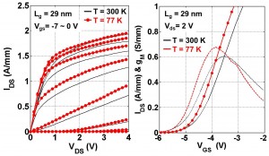
- Figure 1: DC characteristics of 29-nm gate length device at 77 and 300 K.
-
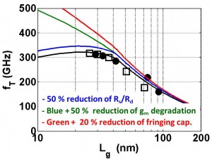
- Figure 2: Comparison between the measurement data and model and estimation of the frequency performance of GaN HEMTs by improving each component.
- K. Shinohara, D. Regan, A. Corrion, D. Brown, S. Burnham, P. J. Willadsen, I. Alvarado-Rodriguez, M. Cunningham, C. Butler, A. Schmitz, S. Kim, B. Holden, D. Chang, V. Lee, A. Ohoka, P. M. Asbeck, and M. Micovic, “Deeply-Scaled Self-Aligned-Gate GaN DH-HEMTs with Ultrahigh Cutoff Frequency,” IEDM Tech. Dig., 2011, paper 19.1, pp. 453-456. [↩]
- D. S. Lee, X. Gao, S. Guo, D. Kopp, P. Fay, T. Palacios, “300-GHz InAlN/GaN HEMTs With InGaN Back-Barrier,” IEEE Electron Dev. Lett., vol. 32, no. 11, pp. 1525-1527, Nov. 2011. [↩]
- Y. Yue, Z. Hu, J. Guo, B. Sensale-Rodriguez, G. Li, R. Wang, f. Faria, T. Fang, B. Song, X. Gao, S. Guo, T. Kosel, G. Snider, P. Fay, D. Jena, H. Xing, “InAlN/GaN HEMTs With Regorwn Ohmic Contacts and fT of 370 GHz,” IEEE Electron Dev. Lett., vol. 33, no. 7, pp. 988-990, July 2012. [↩]
- K. Shinohara, A. Corrion, D. Regan, I. Milosavljevic, D. Brown, S. Burnham, P. J. Willadsen, C. Butler, A. Schmitz, D. Wheeler, A. Fung, and M. Micovic, “220 GHz fT and 400 GHz fmax in 40-nm GaN DH-HEMTs with Re-grown Ohmic,” IEDM Tech. Dig., 2010, paper 30.1, pp. 672-675. [↩]