A Ballistic Transport Model for III-V HEMTs and MOSFETs
- Category: Electronic Devices
- Tags: III-V materials, jesus del alamo, shireen warnock
As silicon metal-oxide-semiconductor field-effect transistors (MOSFETs) keep scaling down in size, fundamental physical limits threaten the continued improvement on their logic performance. With silicon approaching these limits, MOSFETs designed with III-V semiconductors have emerged as promising candidates to replace them. The low-effective mass of various III-V materials such as InGaAs and InAs allow both faster and more power efficient performance[1]. However, one of the key challenges, particularly as devices continue to shrink, is to understand the importance of non-idealities in field-effect transistor (FET) structures. High-electron-mobility transistors (HEMTs) are III-V quantum-well FETs that can be used to explore many issues of relevance to future III-V MOSFETs. HEMTs are worthwhile transistors in their own right, but they are also simpler than III-V MOSFETs and therefore allow a more thorough exploration into the basic transport physics of a quantum-well III-V device.
HEMT experimental data show that electrons travel ballistically at gate lengths of 30-40 nm, suggesting that a ballistic transport model will become only more accurate as channel lengths are scaled down to 10 nm. We investigate to what extent this is true in III-V MOSFETs and also study the impact of short channel effects and other parasitics inherent in a III-V design.
To accomplish these goals, we have developed a flexible transistor model in MATLAB based on a ballistic theory of transport. The model uses, at its core, a one-dimensional, self-consistent Poisson-Schrödinger simulation of the heterostructure of the transistor. We then add extrinsic device parameters such as source and drain parasitic resistances (RS and RD), as well as appropriate values for the drain-induced barrier lowering (DIBL) and a distribution of interface trap states across the band gap at the semiconductor-oxide interface (Dit). We first used HEMTs to calibrate the model’s validity with regards to the current-voltage characteristics. Due to the absence of a gate oxide, HEMTs do not suffer from interface states. We then turned to the physics of relevance to III-V MOSFETs, particularly the effects of Dit on the C-V and I-V characteristics. We can use our model to extract trap density as a function of energy in the bandgap of the barrier semiconductor. Figure 1 shows the C-V curves for a simulated MOSFET structure first with no Dit, and then fitted to an experimental C-V curve using the Dit distribution shown in Figure 2. The MOSFET used for this comparison is an Al2O3 buried-channel device fabricated by Lin et al. and described in[2]. Ultimately, the ability to correctly model and predict device behavior will help identify the problems that need attention in the iterations of future device fabrication.
-
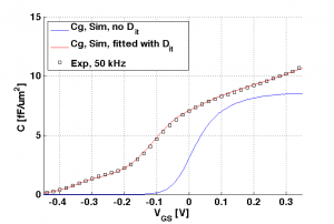
- Figure 1: C-V characteristics of model simulation against experimental data for the long-channel Al2O3 III-V MOSFET in [2], at room temperature. The threshold voltage was fit with I-V sub-threshold characteristics.
-
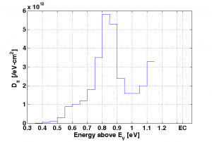
- Figure 2. Dit distribution for III-V MOSFET in [2], extracted from C-V characteristics in Figure 1. The Dit distribution is inside the band gap of the InP barrier layer.
- J. A. del Alamo, “Nanometer-scale electronics with III-V compound semiconductors,” Nature, vol. 479, pp. 317-323, Nov. 2011. [↩]
- J. Lin, D. A. Antoniadis, and J. A. del Alamo, “Sub-30 nm InAs Quantum-Well MOSFETs with Self-aligned Metal Contacts and Sub-1 nm EOT HfO2 Insulator,” IEEE International Electron Devices Meeting, San Francisco, CA, Dec. 10-12, 2012, pp. 757-760. [↩]