category » Electronic Devices
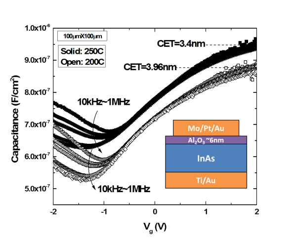
InGaAs-based metal-oxide-semiconductor field-effect transistors (MOSFETs) have shown great potential for future high- performance and low-power logic applications [1] . Superior…
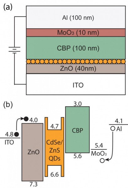
Quantum dot light emitting diodes (QD-LEDs) are promising devices for the next generation of solid-state lighting and other optoelectronic applications….
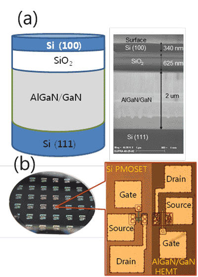
Thanks to their excellent electrical performance, AlGaN/GaN high electron mobility transistors (HEMTs) are considered ideal devices for the next generation…
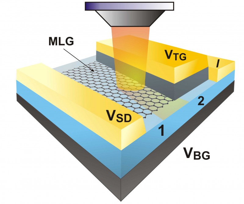
Graphene is a two-dimensional (2D) material that has attracted great interest for electronic devices since its discovery in 2004 [1]…
Nitride-based semiconductors have received considerable attention during the last decade due to their outstanding properties for opto-electronic, high frequency, and…
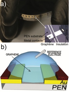
With its all-surface 2D structure combined with very high carrier mobility, graphene is an extremely promising candidate for high sensitivity…
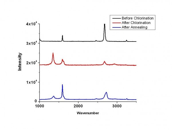
Graphene, a two-dimensional honeycomb lattice of sp2-hybridized carbon atoms, has attracted tremendous interest in the scientific community. Surface functionalization is…
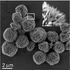
Gas sensors are essential in the monitoring, control, and reduction of harmful emissions in the environment [1] . Conductometric gas…
Detection of high-energy radiation (e.g., γ-rays) is key in nuclear non-proliferation strategies. When a wide-band gap semiconductor detector intercepts a…
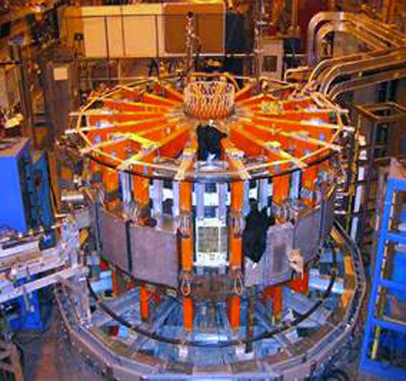
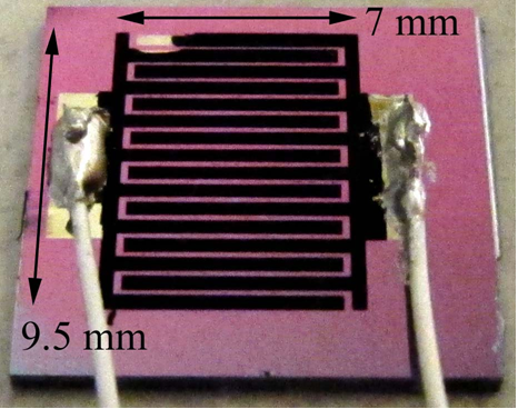
Arrays of MEMS Langmuir probes that are flush-mountable (Figure 1) can serve as a sensorial skin on a spacecraft for…
Development of miniature vacuum pumps that can be integrated with electronic or MEMS components is necessary for producing advanced equipment…
There is an increasing interest in AlGaN/GaN high electron mobility transistors (HEMTs) due to their great potential for high performance…
Epilepsy is a common chronic neurological disorder that affects about 1% of the world population [1] . It is characterized…
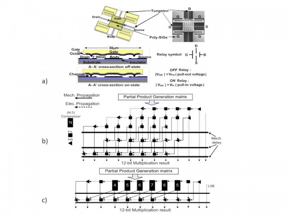
Silicon CMOS circuits have a well-defined lower limit on their achievable energy efficiency due to sub-threshold leakage. Once this limit…
Micro-batteries provide a critical component for self-powered autonomous microsystems. Lithium-ion batteries provide relatively high energy storage capacities. Significant improvement in…
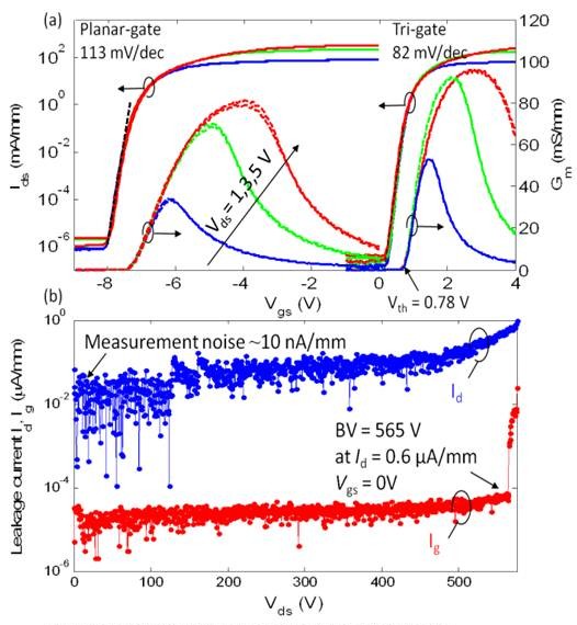
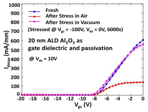
Wide band-gap III-nitride semiconductors have great potential for the next generation of power electronics. GaN high-electron-mobility transistors (HEMTs) in particular…
Two-dimensional crystals, including graphene, hexagonal boron nitride, and transition metal dichalcogenides (TMD) materials, have outstanding properties for developing the next…
We are investigating the fabrication, material, and circuit properties of magnetic memory and logic devices. The research is divided into…
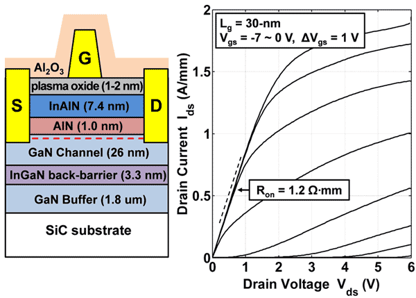
The unique combination of high electron velocity and high breakdown voltage of GaN makes this material an ideal candidate for…
GaN is an excellent material to be used in high-power, high-frequency and high-temperature applications due to its wide band gap,…
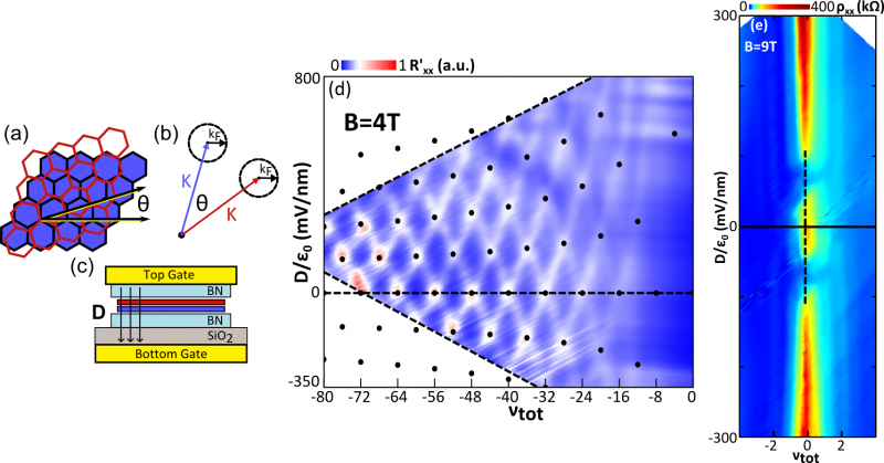
The bilayer 2-dimensional electron gas (2DEG) consists of two closely spaced 2DEGs, between which Coulomb interactions and tunneling effects can…
Due to their mechanical, thermal, and electrical properties and their natural ability to grow on a variety of metallic and…
With the rapid downscaling of CMOS technology, III-V materials have gained much attention due to their high electron mobility. In…
The photoresponse of semiconductors, which determines the performance of optoelectronic devices, is governed by energy relaxation pathways of photoexcited electron-hole…
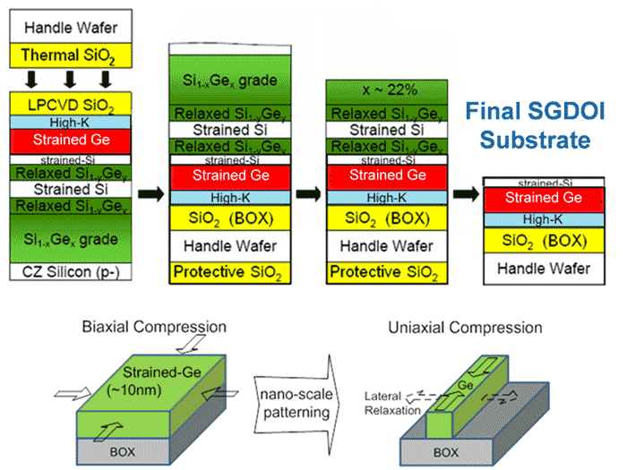
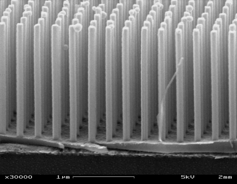
Uniaxial strained Ge “nanobars” are of interest for future sub-10nm gate length p-MOSFETs because of the excellent electrostatic control afforded…
Significant reduction in processor power is needed in order to sustain future data center growth and extend battery life of…
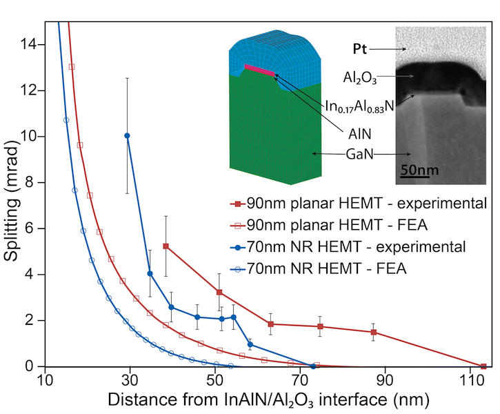
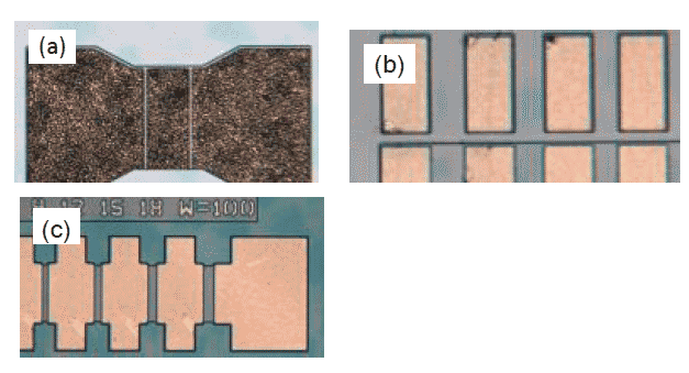
GaN-based high electron mobility transistors (HEMTs) are an important platform for the realization of high-power, high-frequency devices. Nanoribbon (NR) HEMT…
Achieving a sharp subthreshold swing is crucial to enable the supply voltage scaling that is necessary to reducing power consumption…
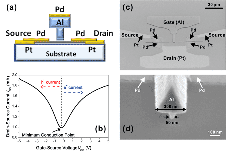
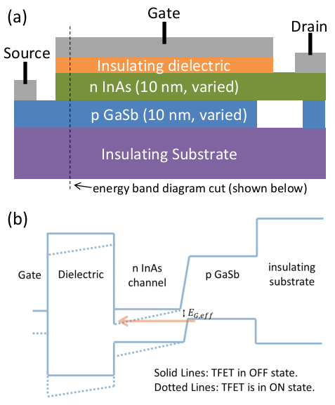
Tunnelling devices based on semiconductor heterojunctions offer the potential for computation with very high energy efficiency. This potential exists because…
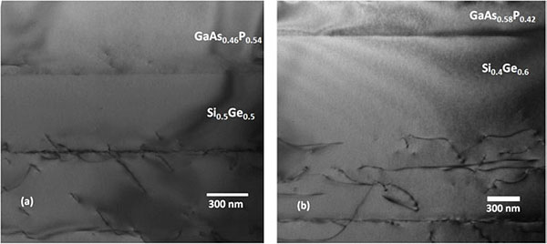
Photovoltaics and sustainability have received much attention lately. We seek a tandem photovoltaic device using silicon as both the substrate…
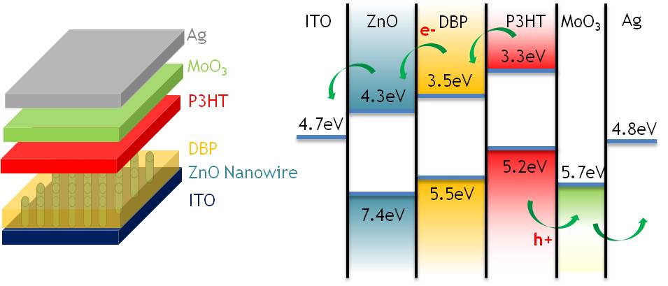
Organic/inorganic hybrid solar cells based on the integration of conductive polymers into semiconducting nanowire arrays offer opportunities for the development…
As CMOS technology continues to scale to the nanometer regime, there has been a strong demand for alternative materials to…
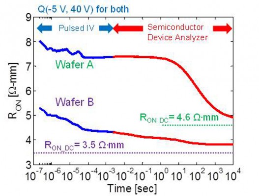
In the last few years, the development of energy-efficient electrical power management systems has received a great deal of interest….
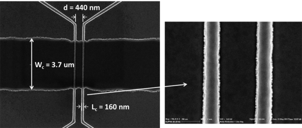
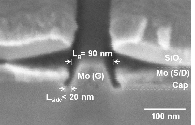
Deeply scaled III-V MOSFETs have demonstrated logic performance at 0.5 V, exceeding that of Si [1] . The gate length…
Nanostructured solar cells are attracting increasing attention as a promising photovoltaic (PV) technology [1] . Generation of free charge carriers…

In this research we seek to develop acousto-optic, guided-wave modulators in proton-exchanged lithium niobate for use in holographic and other…
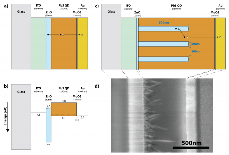
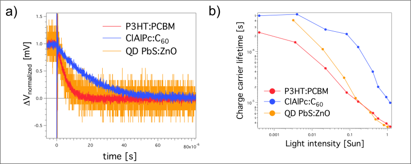
Thin-film solar cells incorporating colloidal quantum dot active layers have recently emerged as a notable third-generation photovoltaic (PV) technology, largely…
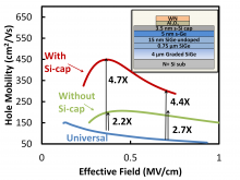
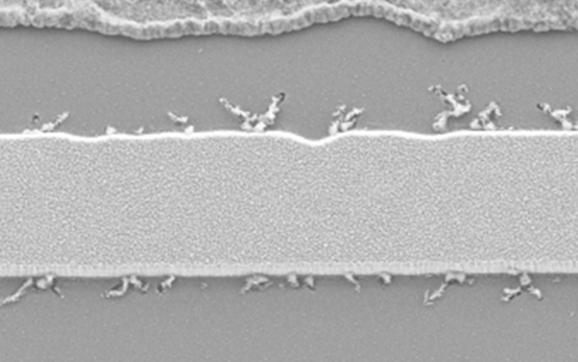
Strained-Ge MOSFETs with significantly enhanced mobility compared to Si/SiO2 hole mobility have previously been reported by our group (see Figure…
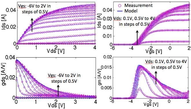
Compact models for GaN based HEMTs describing the voltage-dependent terminal currents are essential for circuit simulations. In this work, we…
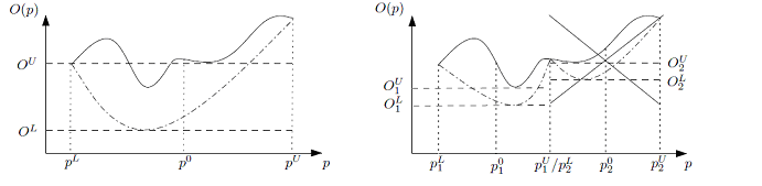
Given recent advances in the field of global optimization, we aim to make advances towards deterministic global optimization of some…
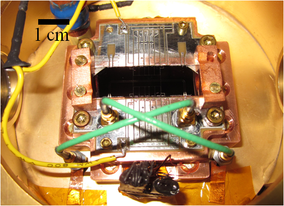
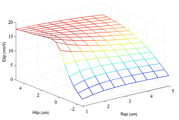
In recent years, several ion-trapping groups have shown that microwave electrodes integrated into surface electrode ion traps can be used…
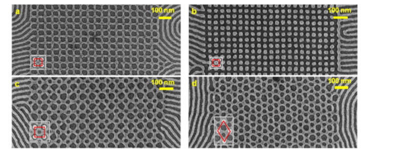
Self-assembled block copolymer structures are useful in nanolithography applications, producing patterns with high resolution and throughput. We previously showed control…
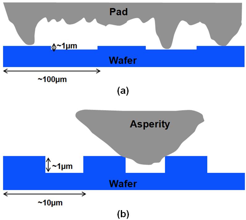
In our previous work on CMP modeling, we developed an original physical die-level model to understand the pattern density dependence…