Dynamic ON-Resistance in High-voltage GaN Field-Effect-Transistors
- Category: Electronic Devices
- Tags: donghyun jin, jesús del alamo
In the last few years, the development of energy-efficient electrical power management systems has received a great deal of interest. Recently, GaN Field-Effect-Transistors have emerged as a disruptive technology with great potential. The high breakdown electric field coupled with the high sheet electron density attainable in GaN heterostructures promises better than three orders of magnitude improvement in the ON-resistance/breakdown-voltage trade-off over conventional Si power-switching devices. However, in spite of recent great progress in GaN power device fabrication technologies, electrical reliability represents a great unknown in these devices. In particular, the dynamic ON-resistance (RON), in which the RON of the transistor remains high for a certain period of time after an OFF-ON switching event, is a big concern [1] . This phenomenon greatly affects the efficiency of electrical power management circuits based on GaN FETs.
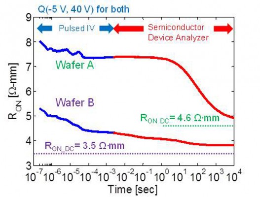
Towards the goal of fundamental understanding on the dynamic ON resistance problem, we have developed a new dynamic RON measurement methodology that allows the observation of RON transients after an OFF-ON switching event from 200 ns to any arbitrary length of time over many decades in time [2] . Using this technique, we have performed a fundamental study of dynamic RON on high-voltage GaN FETs. Figure 1 shows two examples of RON transients obtained over 11 decades in time when the devices are switched from an OFF-state with VGSQ=-5 V and VDSQ=40 V. They are measured by a pulsed IV system (blue lines) and semiconductor device analyzer (red lines) on industrially prototyped AlGaN/GaN HEMTs fabricated on two nominally identical epitaxial wafers (labeled A and B) grown by two different commercial epitaxial vendors. In wafer A, RON at 200 ns is about 73% higher than in DC. For wafer B, RON (200 ns) is about 52% higher than RON_DC. Such a high dynamic RON represents a big problem for power-switching applications. The pattern of recovery of RON is also very different in both wafers. Wafer A exhibits a very slow transient in the s-ks time range, while wafer B recovers on a µs-s time scale. The very different transients obtained in these two wafers suggest that the details of epitaxial growth have a great impact on the dynamics of GaN devices. Figure 2 shows OFF to ON transients from different quiescent VDS values for wafer B. As VDSQ increases, the dynamic RON increases in a prominent manner in both devices, presumably as a result of the increased extension of the high-field region into the drain.
We have carried out additional studies at different temperature and pulse conditions. From all these results, we postulate that on a short time scale, dynamic RON arises from the fast release of electrons from border traps at the AlN/AlGaN interface right above the GaN channel through a tunneling process. In contrast, over a longer time scale, conventional thermally assisted detrapping processes from traps in the AlGaN or at the surface dominate. All of these findings provide a path for proper GaN power-switch device engineering and operation that minimize dynamic RON.
-

- Figure 1: RON transients from 200 ns up to 10,000 s on wafer A and B devices from VGSQ=-5 V, VDSQ=40 V. Blue lines are obtained from pulsed IV system (Auriga AU4750) and red lines from semiconductor device analyzer (Agilent B1500A). Also shown are the DC values of RON obtained after fully detrapping the device.
-
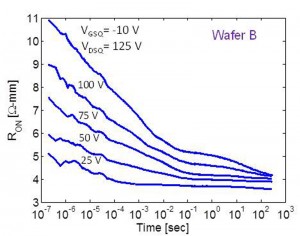
- Figure 2: OFF to ON state transients from different quiescent VDS conditions from VDSQ=25 V up to 125 V in 25 V increments (wafer B device). As VOFF increases, the dynamic RON increases too but the time constants do not change.

- J. A. del Alamo and J. Joh, “GaN HEMT reliability,” Microelectronics Reliability, vol. 49, pp. 1200-1206, September 2009. [↩]
- D. Jin and J. A. del Alamo, “Mechanisms responsible for dynamic ON-resistance in GaN high-voltage HEMTs,” International Symposium on Power Semiconductor Devices and ICs Technical Digest, June 2012. [↩]