Wafer-level Heterogeneous Integration of GaN HEMTs and Si (100) MOSFETs
- Category: Electronic Devices
- Tags: hyung-seok lee, tomas palacios
Nitride-based semiconductors have received considerable attention during the last decade due to their outstanding properties for opto-electronic, high frequency, and high power applications [1] . In addition to this remarkable performance, the high two-dimensional electron gas (2DEG) density and critical electric field of AlGaN/GaN allow a 10-fold increase in the output power density of GaN RF power amplifiers and high voltage electronics, when compared to state-of-the-art GaAs and Si circuits.
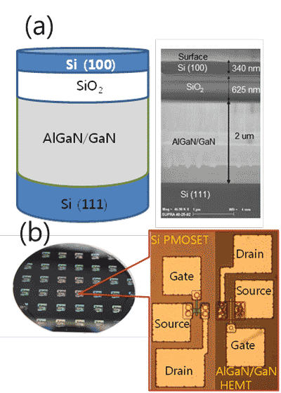
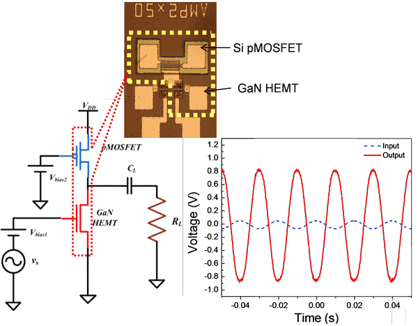
Our group has demonstrated a new technology for the heterogeneous integration of GaN and Si devices, which is scalable at least up to 4” wafers and compatible with conventional Si fabrication. The key step in the proposed technology is the fabrication of a Si (100)-GaN-Si hybrid wafer by bonding a silicon (100) on insulator (SOI) wafer to the nitride surface of an AlGaN/GaN on Si (111) wafer, as shown in Figure 1 (a). A thin layer of silicon oxide is used to enhance bonding between the SOI and AlGaN/GaN wafers. Using this technology, we have fabricated Si pMOSFETs and GaN HEMTs on a 4-inch hybrid wafer (see Figure 1 (b)). Due to the high thermal stability of GaN and the high quality semiconductor material resulting from the transfer method, the devices exhibit excellent performance. A hybrid power amplifier has been fabricated as a circuit demonstrator, which shows the potential to integrate GaN and Si devices on the same chip to enable new performance in high efficiency power amplifiers, mixed signal circuits, and digital electronics. Figure 2 shows a successfully fabricated AlGaN/GaN HEMT voltage amplifier circuit using a Si pMOSFET as a current source. The amplifier has a gain of 17 with 3 V supply voltage, as shown in Figure 2 (right).
-
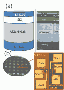
- Figure 1: (a) (left) Simplified schematic cross-sectional view and (right) SEM cross-sectional view of fabricated hybrid wafer. (b) (left) Photograph of a 4-inch hybrid wafer with fabricated GaN-Si devices. (right) Optical micrograph of a Si PMOSFET (Lg=2 μm, W=4 μm) and an AlGaN/GaN HEMT (Lg=2 μm, W=20 μm) fabricated in close proximity.
-
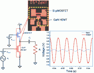
- Figure 2: (left) Schematic of a GaN HEMT voltage amplifier that uses a Si pMOSFET as a current source. (center) An optical micrograph of the hybrid amplifier circuit. (right) Input and output waveforms of the GaN-Si hybrid amplifier.
- D. S. Kuo, C. Shoou-Jinn, T. K. Ko, C. F. Shen, S. J. Hon, and S. C. Hung, “Nitride-based LEDs with phosphoric acid etched undercut sidewalls,” IEEE Photonics Tech. Letters, vol. 21, pp. 510-512, 2009. [↩]