Doping of Graphene Devices through Chlorination
- Category: Electronic Devices
- Tags: graphene, jing kong, mildred dresselhaus, tomas palacios, xu zhang
Graphene, a two-dimensional honeycomb lattice of sp2-hybridized carbon atoms, has attracted tremendous interest in the scientific community. Surface functionalization is a technology to engineer its electronic properties and make it even more desirable and controllable for electronic device applications. For example, chemical functionalization of graphene, especially by hydrogen, fluorine, and chlorine is predicted to enable doping, edge passivation, and opening of its bandgap. Here, we demonstrate that exposure of graphene device to chlorine plasma in an electron cyclotron resonance (ECR) plasma etcher is an effective way to tune the Fermi level of graphene carriers towards p-type direction, without sacrificing its high conductivity.
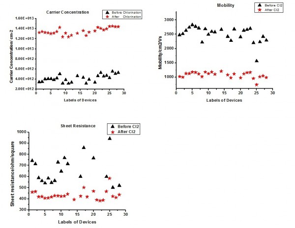
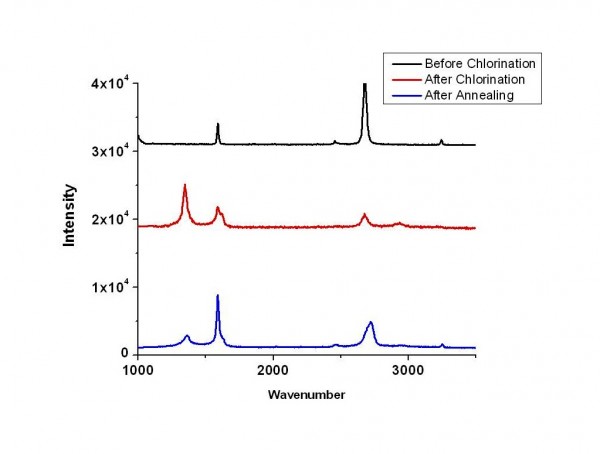
Figure 1 compares the Raman spectroscopy of graphene before and after chlorine plasma treatment and also shows how it changes after annealing. After chlorine plasma treatment for 30 s, the D band increases substantially while the G band blue shift by about 5 cm-1. More importantly, the D band decreases significantly after a 30-min annealing at 500 °C, which means little defect creation occurs during the plasma process. Further transport measurement shows that the carrier concentration in graphene increases considerably. The plasma reaction process tunes the Fermi level of an intrinsic p-type CVD graphene (VDirac >0) towards p-type direction further. We notice that the carrier mobility reduces after plasma reaction. However, this reduction should be mainly due to the increase of hole concentration in graphene rather than defect creation, which is confirmed by the decrease of its sheet resistance and increase of conductivity (see Figure 2). In addition, XPS analysis shows that the percentage of chlorine on the surface of graphene is around 20%. This approach indicates an important way to engineer graphene properties for high-performance applications of graphene devices.
-
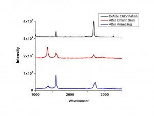
- Figure 1: Raman spectroscopy of graphene before plasma treatment, after plasma treatment, and after annealing.
-
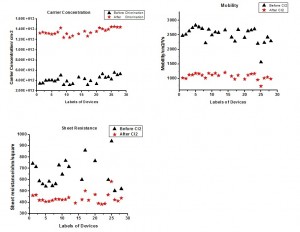
- FIgure 2: Comparison: conductivity, carrier concentration, mobility and sheet resistance of graphene devices before and after chlorination.