Asymmetrically Strained Si/Strained Ge Trigate p-MOSFETs
- Category: Electronic Devices
- Tags: judy l. hoyt, pouya hashemi, winston chern
Uniaxial strained Ge “nanobars” are of interest for future sub-10nm gate length p-MOSFETs because of the excellent electrostatic control afforded by the non-planar device geometry and the potential for high hole velocity in the uniaxial strained Ge. In this work, asymmetrically strained Si/strained Ge trigate p-MOSFETs were fabricated from a strained germanium directly on insulator (SGDOI) substrate. The SGDOI substrate was fabricated using a bond and etchback technique that is depicted in Figure 1. An epitaxial wafer containing the desired final layers was bonded to a thermally oxidized Si handle wafer. The bonded wafer stack is then mechanically ground and chemically etched, leaving the desired final structure with the original grown-in strain intact. The wafer is processed to form p-MOSFETs using hybrid e-beam and photo-lithography to pattern nanobars and source/drain pads, resulting in the final structure seen in the inset of Figure 2. The new free surfaces of the nanobars allow the originally biaxial strain to relax, causing asymmetric strain in the channel of the Ge trigate p-MOSFET. The gate oxide was formed by flowing ozone for passivation and depositing 40A HfO2 and 200A WN as the gate electrode. The gate was used as a mask for ion implantation of boron, and standard CMOS processes was used for metallization. Figure 2 shows the transfer characteristics of a p-MOSFET with 18-nm-wide nanowires.
-
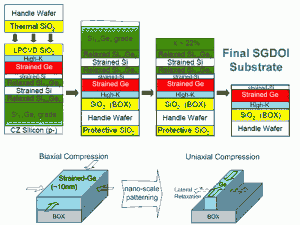
- Figure 1: Schematic of the bond and etchback process for the SGDOI substrate fabrication. After bond and etchback, the film is patterned into a nanobar to induce the biaxial to uniaxial strain transformation.
-
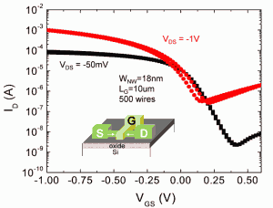
- Figure 2: Transfer characteristics of a strained-Ge trigate with 500, 18nm-wide nanowires in parallel and a gate length of 10um. The sweeps are -50mV (black) and -1V (red). The SS for the device is 83mV/dec, and the hysteresis is ~40mV. The inset illustrates the device schematic.
- P. Hashemi, L. Gomez, M. D. Robertson, M. Canonico, and J. L. Hoyt, “Asymmetric strain in nanoscale patterned strained-Si/strained-Ge/strained-Si heterostructures on insulator,” Applied Physics Letters, vol. 90, no. 8, p. 083109, Aug. 2007.