category » Optics & Photonics

Lack of technology for high-throughput electronic recordings and simultaneous stimulation is a major limiting factor for the development of neuroprosthetics…
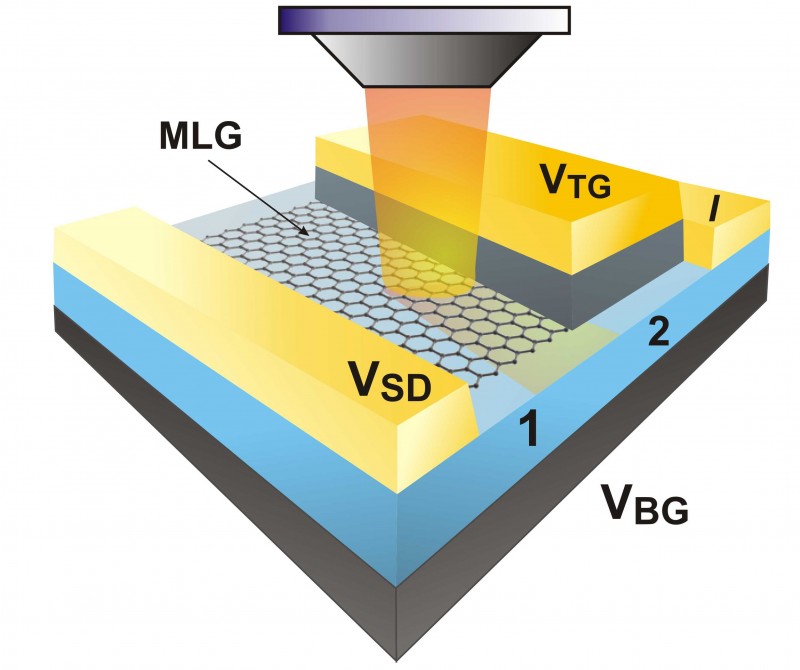
Graphene is a two-dimensional (2D) material that has attracted great interest for electronic devices since its discovery in 2004 [1]…
Silicon photonics is poised to meet the increasing demand for high-bandwidth, low-power, and densely integrated optical communications in CMOS-compatible environments….
High-performance devices and systems based on CMOS-compatible silicon photonics are increasingly gaining momentum in the optical interconnects community as essential…
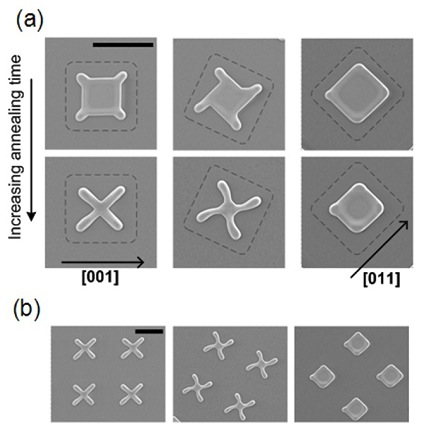
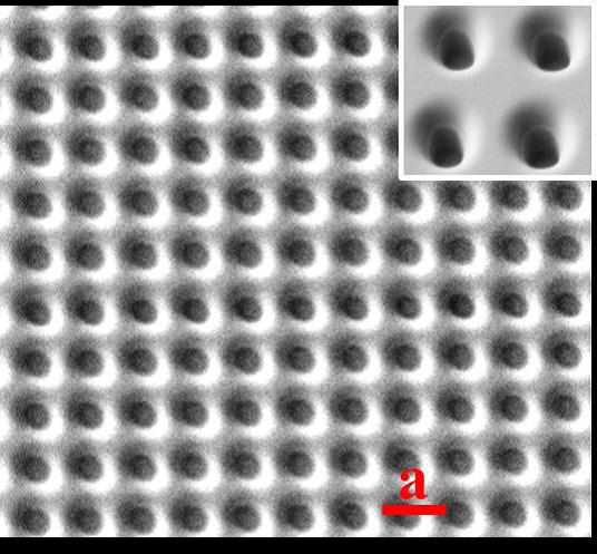
Because thin films are usually unstable in the as-deposited state, at sufficiently high temperatures atomic motion will occur and lead…
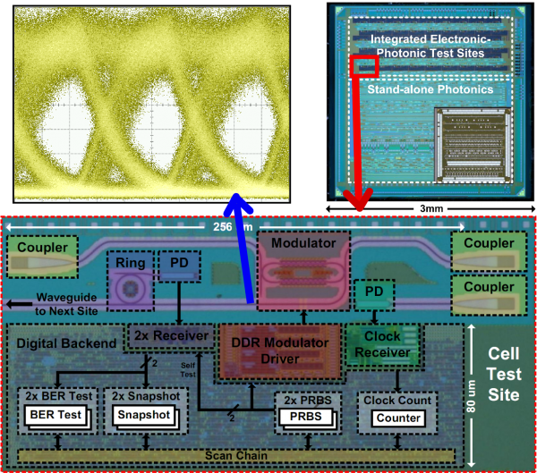
Integrated photonic interconnects present a disruptive alternative to electrical I/O for many VLSI applications, with potential for superior bandwidth density…
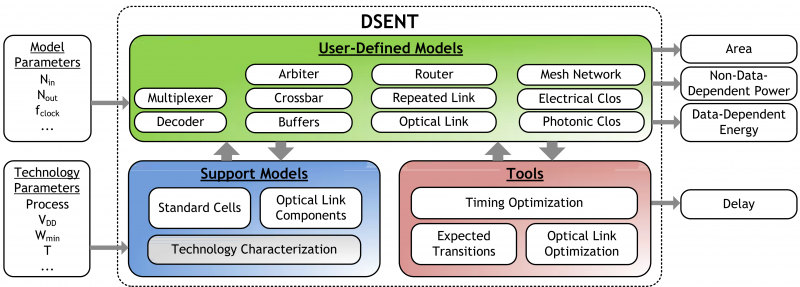
With the rise of many-core chips that require substantial bandwidth from the network-on-chip (NoC), integrated photonic links have been investigated…
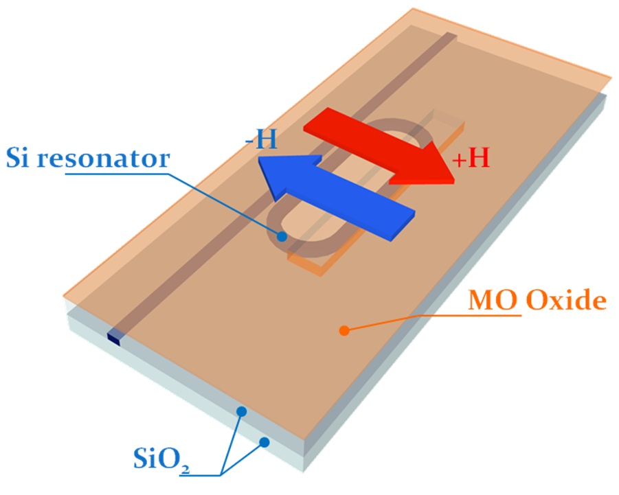
We have experimentally demonstrated a monolithically integrated ultra-compact optical isolator on silicon. This device allows a significant device footprint reduction…
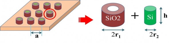
Solar cells with broadband absorption and large acceptance angle are demonstrated by using two-dimensional core-shell structures, which are composed of…
Two-dimensional photonic crystals (PhCs) are fabricated using dual-beam focused ion beam (FIB) in Er3+-TeO2 thin films and demonstrate broadband enhancement…
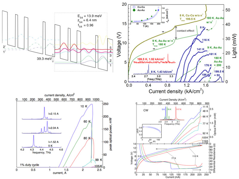
The terahertz frequency range (1-10 THz) has long remained undeveloped, mainly due to the lack of compact, coherent radiation sources….
The photoresponse of semiconductors, which determines the performance of optoelectronic devices, is governed by energy relaxation pathways of photoexcited electron-hole…
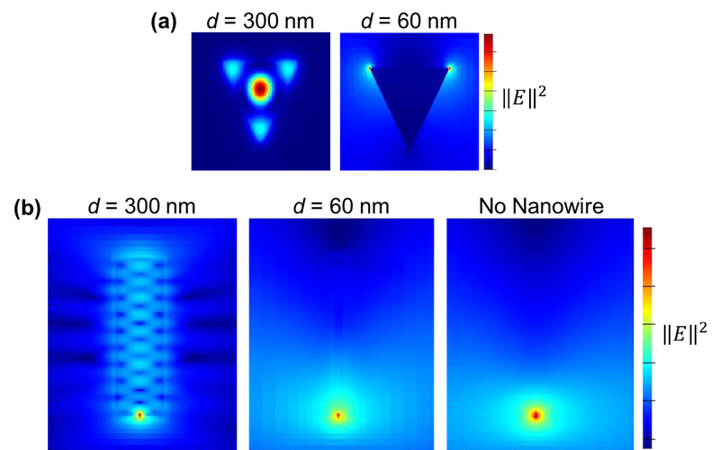
Nanowires are an exciting architecture for light emitting diodes (LEDs). To address the challenges of solid state lighting, III-V nitride…
Optogenetics is commonly used for precision modulation of the activity of specific neurons within neural circuits [1] , but assessing…
We have demonstrated for the first time in-plane InGaAs/InP laser diodes recess-integrated with SiON waveguides on silicon substrates using a…
The use of magnetic forces to improve fluidic self-assembly of micro-components has been investigated using Maxwell 3D to model the…
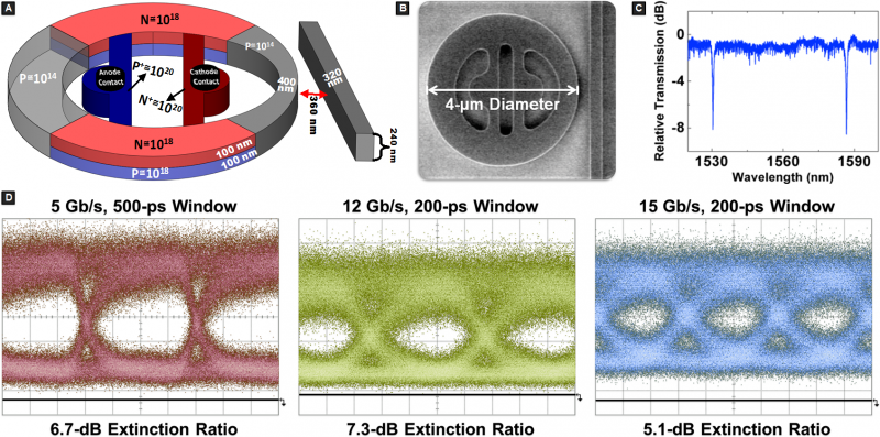
Optoelectronic devices intimately integrated on silicon integrated circuits have long been sought for optical intercon-nect applications, optical communications modules, and–more…

Professor Ed Boyden uses light to precisely control neural activity. His lab has invented safe, effective ways to deliver light-gated…

The cost of silicon solar cells has fallen precipitously in recent years, primarily as a result of manufacturing improvements, increasing…

In this research we seek to develop acousto-optic, guided-wave modulators in proton-exchanged lithium niobate for use in holographic and other…
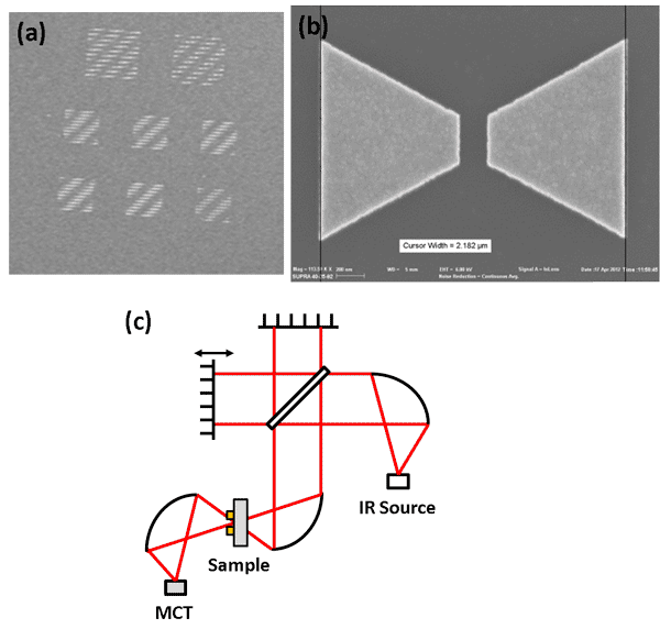
Photolithography’s accuracy and scalability have made it the method for sub-micron-scale definition of single-crystal semiconductor devices for over half a…
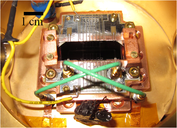
We report on the detection of single-photons in the middle-infrared (mid‑IR) range using superconducting nanowire single-photon detectors (SNSPDs). In 2011…
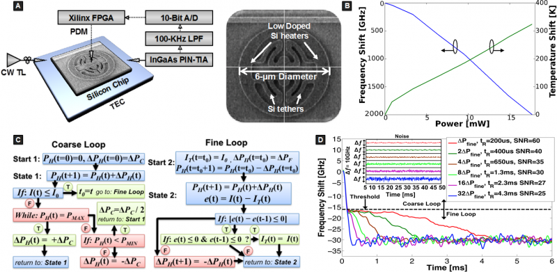
In recent years, several ion-trapping groups have shown that microwave electrodes integrated into surface electrode ion traps can be used…
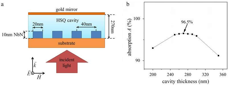
Superconducting nanowire single-photon detectors (SNSPDs) [1] , based on 100-nm-wide, ~ 4-nm‑thick niobium nitride (NbN) nanowires, are unmatched in sensitivity [2]…
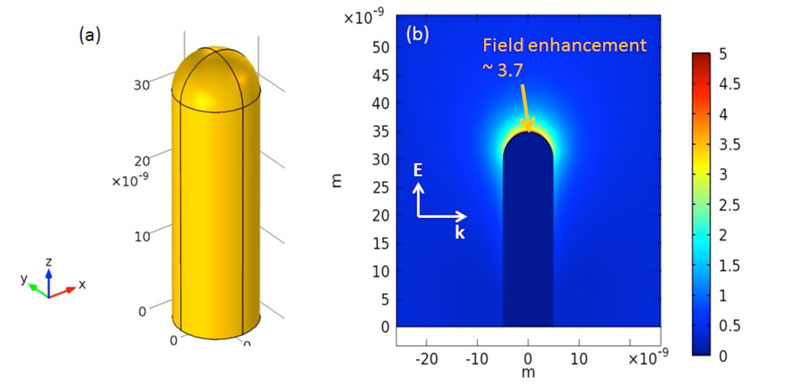
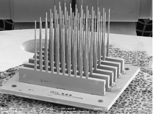
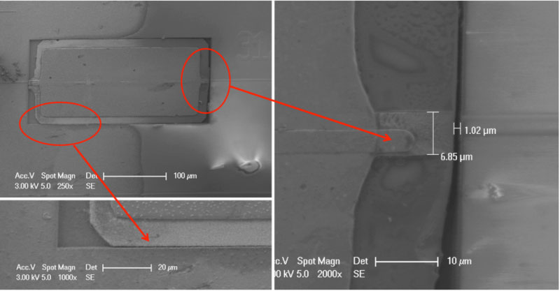
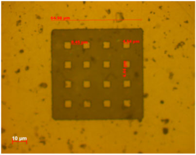
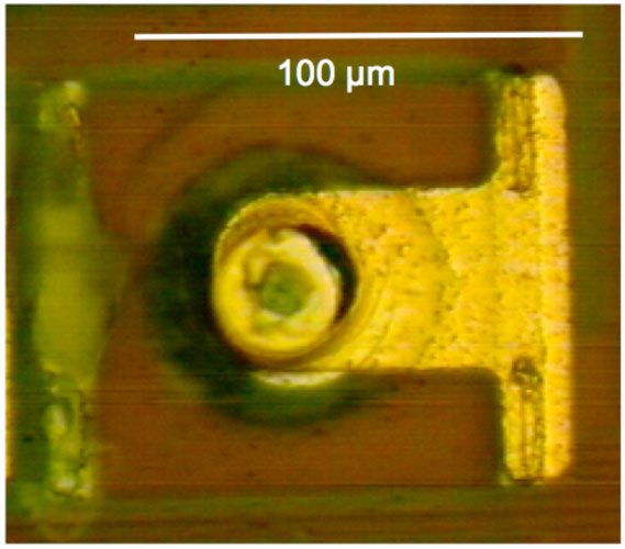
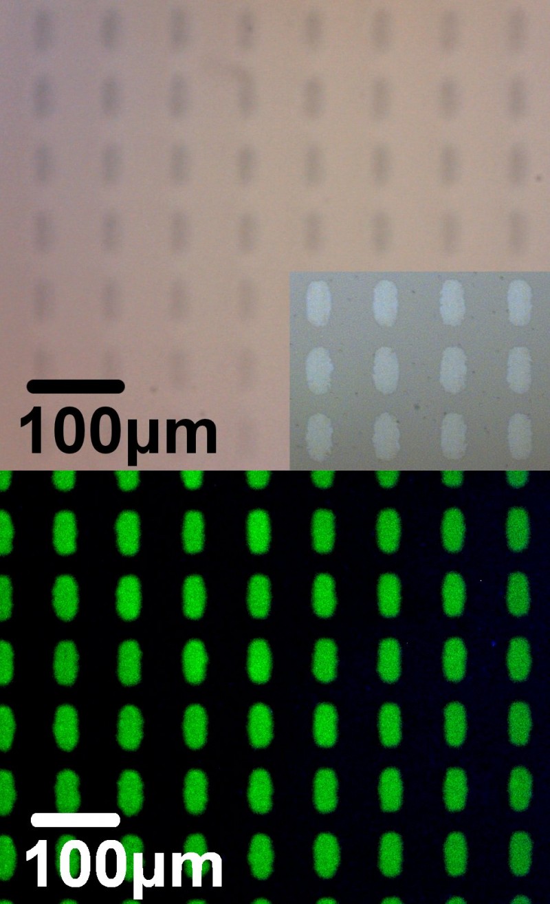
We are interested in the application of arrays of electron field emitters, which can be achieved from a variety of…
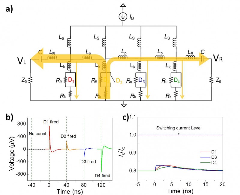
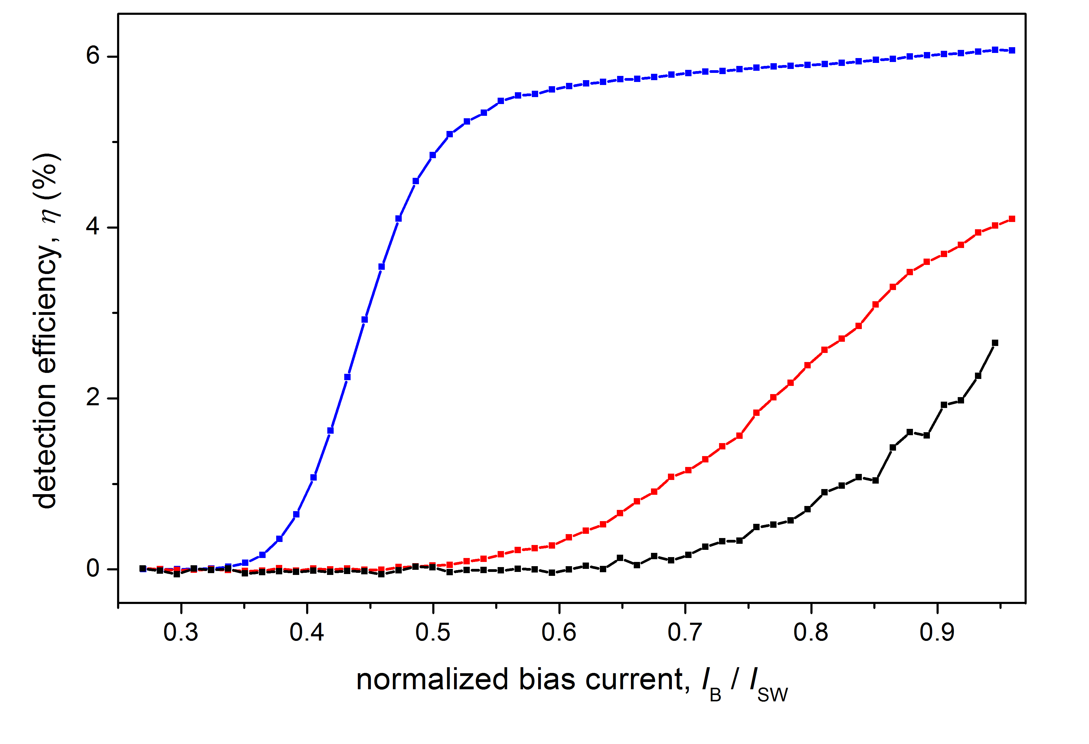
Single pixels of superconducting nanowire single photon detector (SNSPD) have high detection efficiency, low dark-count rate, and low timing jitter….