MOS Interfaces in the InAs/GaSb System
- Category: Electronic Devices
- Tags: iii-v materials, judy l. hoyt, tao yu
With the rapid downscaling of CMOS technology, III-V materials have gained much attention due to their high electron mobility. In particular, indium-arsenide and gallium-antimonide are becoming more popular due to their matched lattice constant and their complimentary physical properties, such as bandgap and carrier mobility [1] ; various heterostructure-based high performance field-effect transistors (FET) and tunneling transistors have been proposed [1] [2] . On the other hand, this material system faces challenges due to the poor oxide/semiconductor interface, which results in high interface trap concentration (Dit) and hence Fermi-level pinning [3] [4] . Therefore, understanding the metal-oxide-semiconductor (MOS) interface in this material system is critical. This study investigates atomic-layer-deposited (ALD) Al2O3 on InAs to provide a preliminary understanding of the Al2O3/InAs interface.
On an S-doped n-type InAs substrate, 60 cycles of Al2O3 are deposited at 200°C and 250°C after HCl wet chemical cleaning. Then, a Mo/Pt/Au (30 nm/20 nm/100 nm) gate stack is formed using electron-beam evaporation; the back contact is formed using Ti/Au. Finally, 30s post-metallization annealing in N2 is carried out. Figure 1 shows the normalized capacitance-voltage (C-V) curves of both samples with frequencies varied from 10kHz to 1MHz. The depletion region of the C-V curve is not sharp and deep, as predicted by simulations [5] , which is mainly due to the series capacitance corresponding to Dit. Still, the comparison between the two samples shows that Al2O3 deposited at 200°C yields lower Dit than 250°C. Figure 2 plots the C-V hysteresis of the two samples at 100kHz, which reflects the oxide mobile charge near the interface. The results show that the hysteresis is moderate for both samples and that the ALD dielectric quality is promising. Quantitative analysis of the Dit is ongoing. In summary, InAs/GaSb is a promising heterojunction system, and research is needed to better understand and optimize the dielectric/semiconductor interface.
-
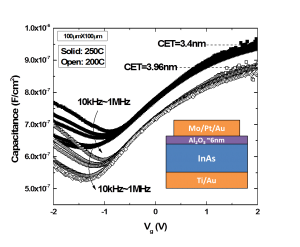
- Figure 1: C-V curves of InAs MOSCAP with Al2O3 dielectric deposited at 200°C and 250°C. Higher deposition temperature gives slightly higher dielectric constant of the dielectric. Impact of Dit induced series capacitance dominates the depletion behavior of both samples.

-
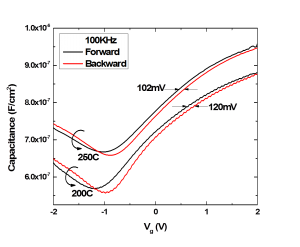
- Figure 2: Hysteresis in C-V characteristics of both samples at 100KHz. Mobile charge control in both samples is promising, with hysteresis ~100mV.
- H. Kroemer, “The 6.1 Å family (InAs, GaSb, AlSb) and its heterostructures: A selective review,” Physica E: Low-dimensional Systems and Nanostructures, vol. 20, no. 3–4, pp. 196–203, Jan. 2004. [↩] [↩]
- B. R. Bennett, R. Magno, J. B. Boos, W. Kruppa, and M. G. Ancona, “Antimonide-based compound semiconductors for electronic devices: A review,” Solid-State Electronics, vol. 49, no. 12, pp. 1875–1895, Dec. 2005. [↩]
- H.-D. Trinh, E. Y. Chang, Y.-Y. Wong, C.-C. Yu, C.-Y. Chang, Y.-C. Lin, H.-Q. Nguyen, and B.-T. Tran, “Effects of wet chemical and trimethyl aluminum treatments on the interface properties in atomic layer deposition of Al2O3 on InAs,” Japanese Journal of Applied Physics, vol. 49, no. 11, p. 111201, Nov. 2010. [↩]
- H.-Y. Lin, S.-L. Wu, C.-C. Cheng, C.-H. Ko, C. H. Wann, Y.-R. Lin, S.-J. Chang, and T.-B. Wu, “Influences of surface reconstruction on the atomic-layer-deposited HfO2/Al2O3/n-InAs metal-oxide-semiconductor capacitors,” Applied Physics Letters, vol. 98, no. 12, p. 123509, 2011. [↩]
- D. Wheeler, L.-E. Wernersson, L. Fröberg, C. Thelander, A. Mikkelsen, K.-J. Weststrate, A. Sonnet, E. M. Vogel, and A. Seabaugh, “Deposition of HfO2 on InAs by atomic-layer deposition,” Microelectronic Engineering, vol. 86, no. 7–9, pp. 1561–1563, Sep. 2009. [↩]