Novel Semiconductor Heterostructures for Tunneling Devices
- Category: Electronic Devices, Materials
- Tags: eugene fitzgerald, ryan iutzi
Tunnelling devices based on semiconductor heterojunctions offer the potential for computation with very high energy efficiency. This potential exists because devices that utilize quantum tunnelling as a switching mechanism are not limited in the sharpness of their turn-on, in contrast to thermally activated devices such as MOSFETs, whose turn-on is limited due to a minimum possible subthreshold slope of 60 mV/decade. In the past few years, much work has focused on InAs/AlGaSb heterojunctions [1] due to their type-III band alignment. While simulations have shown the potential for excellent subthreshold slopes, there has been limited experimental work to date to determine if these devices can actually achieve strong performance in light of the many materials aspects that cannot be accounted for in simulation.
Our work focuses on understanding the materials properties of tunnelling heterojunctions, how they affect device performance, how they can be controlled from a processing perspective, and how they affect device performance. Specifically, we are exploring the various defects present in InAs/AlGaSb heterojunctions and how they can be minimized. We have found that these structures are highly sensitive to the nature of the interface, with certain interface types leading to metallic structures that inhibit growth or significant dislocation densities, which may weaken device performance. We have developed techniques to minimize these defects.
Additionally, we are exploring alternatives to Sb-based devices; specifically heterojunctions utilizing InAs and Ge. We have developed processes to epitaxiallly grow these materials together with varying Ge dimensionalities including 0D (Ge quantum dots), 1D (Ge nanowires), and 2D/3D (Ge thin film). We are currently assessing the various materials defects present in these highly-strained structures, such as dislocations and stacking faults, and how they affect device performance.
-
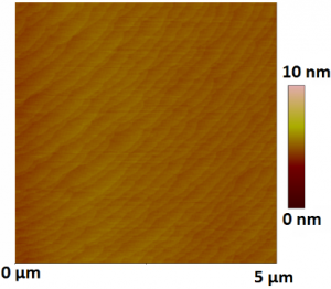
- Figure 1: Atomic force microscopy (AFM) image of epitaxially regrown GaSb, with atomic steps apparent on the surface and no defects.

-

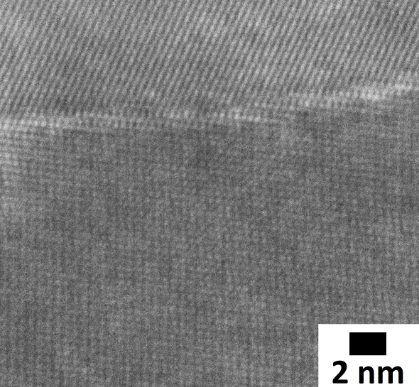
- Figure 2: Lattice-resolved transmission electron microscopy (TEM) image of Ge grown on top of a (100) InAs surface, offcut 6° towards (110), with (100) facets visible.
- A. C. Seabaugh and Q. Zhang, “Low-voltage tunnel transistors for beyond CMOS logic,” Proceedings of the IEEE, 2010, vol. 98, pp. 2095-2110. [↩]