Superlattice-Source Nanowire FET with Steep Subthreshold Characteristics
- Category: Electronic Devices, Energy, Materials, Nanotechnology
- Tags: jesús del alamo, xin zhao
Achieving a sharp subthreshold swing is crucial to enable the supply voltage scaling that is necessary to reducing power consumption in logic field-effect transistors. In this research, we are investigating a new approach to accomplish this swing based on nanowire FETs with a band engineered superlattice source (SLS).
A steep-subthreshold swing (S) in an FET requires suppressing the subthreshold regime, which in essence is the injection of relatively high-energy source electrons above the energy barrier with the channel. A way to accomplish this injection is to create a miniband in the source with a minigap above it, where no states are allowed. If appropriately designed, no current is possible until the top of the source miniband lines up with the conduction band edge in the channel. The transition between the ON state and the OFF state can be quite sharp, and the attainable ON current can reach a value comparable to that of a regular FET. In theoretical calculations performed by Gnani et al [1] , they have concluded that a variety of SLs can accomplish these goals: AlGaAs/GaAs, InAlAs/InGaAs, and AlGaN/GaN, among others. These are short period SLs with barriers and wells in the 1-2 nm regime. Furthermore, 7 periods appears to be enough to accomplish the filtering action of the SL. They have shown that values of S in the 10-20 mV/dec are possible (at 300K).
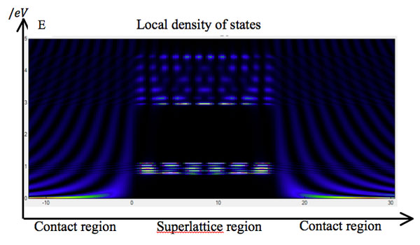
Our goal is to demonstrate a prototype SLS NW-FET in the InAlAs/InGaAs system and to study its suitability for steep-subthreshold and ultra-low voltage operation. The proposed device will be a vertical nanowire transistor with superlattice region incorporated in the source. In order to design a suitable heterostructure and device architecture, we created a simulation environment for the miniband structure of superlattices in various material systems using Nextnano. Based on a built-in 1D ballistic transport model, the local density of states was calculated to show explicitly the miniband position, as in Figure 1. Our calculations indicate that a demanding nanowire diameter of sub-10 nm is needed to achieve single transversal sub-band behavior.
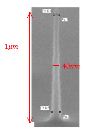
In our quest for nanowire FETs, we are developing a reactive ion etch (RIE) process for InGaAs/InAlAs nanowires. Using HSQ as the hard mask defined by electron beam lithography, we have shown promising etch results using Cl2 based chemistry, as in Figure 2. This will follow with planarization to provide a contact to the top of the nanowire.
-
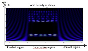
- Figure 1: Local density of states of InAlAs/InGaAs superlattice showing miniband/minigap structure. The simulation was done using the contact block reduction method.
-
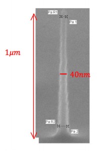
- Figure 2: High aspect ratio RIE etch of GaAs wafer.
- E. Gnani, P. Mariorano, S. Reggiani, A. Gnudi, G. Baccarani, “Investigation on superlattice heterostructures for steep-slope nanowire FETs,”, Device Research Conference, 2011, pp. 201-202. [↩]