2D Crystals for Ubiquitous Electronics
- Category: Circuits & Systems, Electronic Devices, Nanotechnology
- Tags: han wang, jing kong, tomas palacios
Two-dimensional crystals, including graphene, hexagonal boron nitride, and transition metal dichalcogenides (TMD) materials, have outstanding properties for developing the next generation of electronic devices [1] [2] . Graphene is the first 2D crystal to attract attention. The symmetry of its honeycomb lattice structure confers on it unique transport properties. The advantages of graphene for radio-frequency (RF) applications derive in part from its high electron and hole mobility, which can exceed 200,000 cm2/Vs at T=5 K and 100,000 cm2/Vs at T=240 K [3] [4] , the highest ever reported for any semiconductor. Moreover, graphene is a zero-bandgap material in which the conduction and valence bands touch at a point called the Dirac point. In addition to zero bandgap, the density of states in graphene is zero at the Dirac point and increases linearly for energies above and below it, which allows for carrier modulation. The carriers in graphene are confined to a one-atom-thick layer, allowing unprecedented electrostatic confinement and making graphene flexible and transparent. The lack of bandgap can be compensated for by integrating it with other 2D materials such as MoS2from the TMD family [5] [6] . MoS2 shares many of graphene’s advantages for electronic applications; its 1.8 eV bandgap makes it ideal for building logic circuits to complement graphene.
This project demonstrates important building blocks for future integrated circuits based on 2D-materials on flexible substrates such as plastics, paper and textiles. These basic analog building blocks include ambipolar frequency multipliers [7] [8] , graphene RF mixers [9] , graphene oscillators, and graphene phased shift keying devices, plus technology for fabricating flexible devices and circuits on plastic substrates. We construct integrated logic circuits based on few-layer MoS2, including an inverter, a NAND gate, a memory device, and a ring oscillator. Prototypes of these building blocks move towards new technologies that seamlessly integrate electronics into objects of daily life, from plastic and paper cups with integrated temperature sensors and clothing with embedded RF antennas to smart contact lenses that communicate with cell phones to display relevant information to the wearer.
-
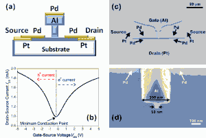
- Figure 1: (a) Schematic of the graphene FET device structure. (b) ambipolar IDS-VGS characteristics of the fabricated GFET. (c) SEM image of the device. (d) SEM image of the T-shape gate of a self-aligned graphene transistor.
-
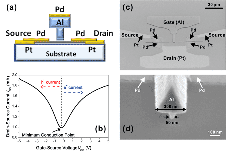
- Figure 2: (a) Application circuit of graphene frequency multipliers. (b) input (red) and output (black) signals of 6-GHz graphene frequency multiplier. (c) output signal spectrum of graphene RF mixer. (d) output spectrum of a graphene electrical oscillator.
- A. K. Geim, “Graphene: Status and prospects,” Science, vol. 324, no. 5934, pp. 1530-1534, June 2009. [↩]
- A. H. C. Neto, et. al., “The electronic properties of graphene,” Rev. Mod. Phys., vol. 81, pp. 109–162, 2009. [↩]
- K. I. Bolotin, et al., “Ultrahigh electron mobility in suspended graphene,” Solid State Communications, vol. 146, no. 9, June 2008. [↩]
- K. I. Bolotin, et al., “Temperature-dependent transport in suspended graphene,” Phys. Rev. Lett., vol. 101, 096802, 2008. [↩]
- P. Joensen, R. F. Frindt, and S. R. Morrison, “Single-layer MoS2” Mat. Res. Bull., vol. 21, pp. 457-461, 1986. [↩]
- B. Radisavljevic, et. al., “Single-layer MoS2 transistors,” Nature Nanotechnology, vol. 6, pp. 147–150, 2011. [↩]
- H. Wang, D. Nezich, J. Kong, and T. Palacios, “Graphene frequency multipliers,” IEEE Electron Device Lett., vol. 30, no. 5, May 2009. [↩]
- H. Wang, et. al., “Gigahertz ambipolar frequency multiplier based on CVD graphene,” IEDM Tech. Digest, vol. 23, no. 6, pp. 572-575, 2010. [↩]
- H. Wang, et. al., “Graphene-based ambipolar RF mixers,” IEEE Electron Device Lett., vol. 31, no. 9, Sept. 2010. [↩]