Silicon Field Emitter Arrays for Chip-scale Vacuum Pumping
- Category: Electronic Devices, MEMS & BioMEMS, Nanotechnology
- Tags: akintunde akinwande, arash fomani, luis velasquez-garcia
Development of miniature vacuum pumps that can be integrated with electronic or MEMS components is necessary for producing advanced equipment such as portable analytical instruments [1] and high performance sensors [2] . The proposed approach graphically illustrated in Figure 1 is based on electron impact ionization (EEI) or field ionization (FI) of the gas molecules using nano-scale sharp silicon tips. The ionized gas molecules are then evacuated from the chamber using a strong electric field to accelerate the ions and implant them permanently into a getter medium made of Ti or Al. In the EEI mode of the operation, a positive voltage is applied between the gate and the emitter to extract electrons that are used to ionize the background gas. In the FI regime, the Si sharp tips are biased at a positive voltage with respect to the gate to extract electrons from the outer shell of the gas molecules in a quantum tunneling process. The former process occurs at electric fields in the range of 3 – 6 ×10⁷ V/cm while the later process initiates at electric fields above 108 V/cm [3] . Despite the larger required voltage, the operation in the FI regime is mandatory since the back-streaming of the positive ions during EEI mode of operation will damage the field emitter (FE) tips at mTorr-pressure range. Although state-of-the-art field emitters have been reported [4] [5] [6] , the focus of this work is to improve the reliability of the FE or FI devices for extended operation times and large currents necessary for pumping application. Since these devices demand application of large voltages between the gate and the tip of the FE/FI, wear or breakdown of the insulating dielectric is a major issue. Finite element modeling (shown in Figure 2) has been conducted to optimize the design of the device for pumping application. A new fabrication process is also being developed for high-yield fabrication of an array with more than 300K Si FEs/FIs.
-
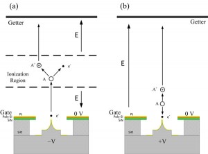
- Figure 1: Evacuation of gas molecules using (a) electron impact ionization and (b) field ionization mechanisms.
-
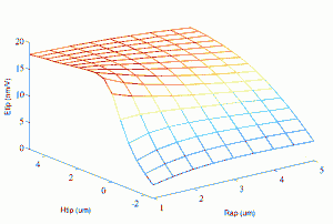
- Figure 2: Electric filed at the tip of a Si FE/FI as a function of gate aperture radius and tip distance from the gate plane (V = 300V).
- Z. Ouyang and R. G. Cooks, “Miniature mass spectrometers,” Annual Review of Analytical Chemistry, vol. 2, pp. 187-214, Feb. 2009. [↩]
- M. Esashi, “Wafer level packaging of MEMS,” Journal of Micromechanics and Microengineering, vol. 18, no. 7, pp. 073001:1-13, May 2008. [↩]
- R. Gomer, Field Emissions and Field Ionization, New York: Springer-Verlag, Dec. 1992. [↩]
- M. Ding, G. Sha, A. I. Akinwande, “Silicon field emission arrays with atomically sharp tips: turn-on voltage and the effect of tip radius distribution,” IEEE Transaction on Electron Devices, vol. 49, no. 12, pp. 2333-2342, Dec. 2002. [↩]
- L. F. Velásquez-García, S. A. Guerrera, Y. Niu, and A. I. Akinwande, “Uniform high-current cathodes using massive arrays of Si field emitters individually controlled by vertical Si ungated FETs – part 1: Device design and simulation,” IEEE Transactions on Electron Devices, vol. 58, no. 6, pp. 1775-1782, June 2011. [↩]
- L. F. Velásquez-García, S. A. Guerrera, Y. Niu, and A. I. Akinwande, “Uniform high-current cathodes using massive arrays of Si field emitters individually controlled by vertical Si ungated FETs – part 2: Device fabrication and characterization,” IEEE Transactions on Electron Devices, vol. 58, no. 6, pp. 1783-1791, June 2011. [↩]