300-GHz GaN Transistors
- Category: Electronic Devices
- Tags: dong seup lee, gallium nitride, tomas palacios
The unique combination of high electron velocity and high breakdown voltage of GaN makes this material an ideal candidate for high power and high frequency applications. Among the different possible nitride structures, an InAlN/GaN heterostructure is one of the most promising candidates for high frequency applications because the large polarization discontinuity between InAlN and GaN induces an extremely large charge density with barriers thinner than 10 nm.
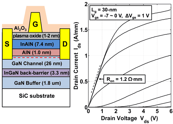
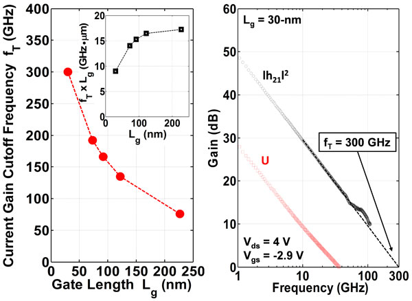
This work reports lattice-matched In0.17Al0.83N/GaN high electron mobility transistors (HEMTs) on a SiC substrate with a record current gain cutoff frequency (fT) of 300 GHz [1-2]. To suppress short-channel effects (SCEs), an In0.15Ga0.85N back-barrier is applied in an InAlN/GaN heterostructure for the first time. The GaN channel thickness is also reduced to 26 nm, which allows a good immunity to SCEs for gate lengths down to 70 nm, even with a relatively thick top barrier (9.4-10.4 nm). In a device with a gate length (Lg) of 30 nm, an on-resistance (Ron) of 1.2 Ω•mm, and an extrinsic transconductance (gm.ext) of 530 mS/mm, a peak fT of 300 GHz is achieved. An electron velocity of 1.37-1.45×107 cm/s is extracted by two different delay analysis methods.
-
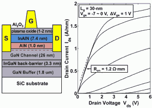
- Figure 1: (a) Cross-sectional schematic of an InAlN/GaN HEMT with an InGaN back-barrier. (b) Ids-Vds characteristics of the devices with Lg = 30 nm.
- D. S. Lee, X. Gao, S. Guo, D. Kopp, P. Fay, and T. Palacios, “300-GHz InAlN/GaN HEMTs with InGaN back-barrier,” IEEE Electron Device Letters, vol. 32, no. 11, pp. 1525-1527, Nov. 2011.
- D. S. Lee, B. Lu, M. Azize, X. Gao, S. Guo, D. Kopp, P. Fay, and T. Palacios, “Impact of GaN channel scaling in InAlN/GaN HEMTs,” IEDM Technical Digest 2011, pp. 457-460, Dec. 2011.