Stress State Characterization of InAlN/GaN Nanoribbon HEMT Structures using Convergent Beam Electron Diffraction
- Category: Electronic Devices, Materials, Nanotechnology
- Tags: eric jones, mohamed azize, silvija gradecak, tomas palacios
GaN-based high electron mobility transistors (HEMTs) are an important platform for the realization of high-power, high-frequency devices. Nanoribbon (NR) HEMT structures represent a novel route towards piezodoping by allowing external stresses to be applied in the plane of the active layer and have been shown to enhance carrier transport properties [1] . This work uses transmission electron microscopy (TEM) and finite element analysis (FEA) to investigate the stress state of InAlN/GaN NR HEMT devices and explore the role of Al2O3 in stress generation.
NR structures were fabricated using top-down techniques and passivated with varying thicknesses of Al2O3. TEM samples were obtained from the device structures by using focused ion beam techniques. Using convergent beam electron diffraction, strain relaxation profiles were obtained by analyzing the splitting of higher order Laue zone lines contained in the [5 4 0] zone axis pattern. Splitting profiles were also generated from FEA models of the HEMT structure for comparison. Finally, device-sized structures were simulated to investigate the stress state of the active HEMT layers as a function of the oxide thickness.
Comparison of the experimental and simulated splitting profiles in Figure 1 shows not only that the FEA model correctly replicates overall splitting behavior and the dependence on sample thickness, but that it also consistently under-estimates the experimental results, suggesting an additional source of stress not present in the current model. Models of device structures showed a compressive stress generated in the active HEMT layer upon the creation of a NR structure that becomes tensile when a layer of Al2O3 is applied, as shown in Figure 2. The magnitude of the tensile stress approaches that of the planar structure as the thickness of the oxide increases. This data correlates well with earlier published [1] electrical characterization of these structures considering the decrease in carrier concentration observed for a compressive strain [2] .
-
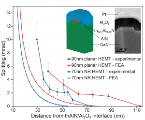
- Figure 1: Comparison of experimental splitting profiles obtained using CBED and simulated profiles from FEA. Insets show dark-field scanning TEM image and schematic model of NR structure.
-
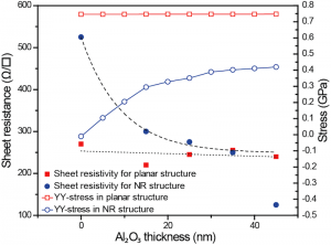
- Figure 2: Stress in the active HEMT layer for both NR and planar structures as a function of oxide thickness calculated using FEA compared to sheet resistance data replotted from [1] .

- M. Azize, A. L. Hsu, O. I. Saadat, M. Smith, X. Gao, S. P. Guo, S. Gradečak, and T. Palacios, “High-electron-mobility transistors based on InAlN/GaN nanoribbons,” IEEE Electron Device Letters, vol. 32, pp. 1680-1682, Dec 2011. [↩] [↩] [↩]
- J. Kuzmik, “InAlN/(In)GaN high electron mobility transistors: Some aspects of the quantum well heterostructure proposal,” Semiconductor Science and Technology, vol. 17, pp. 540-544, June 2002. [↩]