Technology Development for GaN and Si Integration
- Category: Electronic Devices
- Tags: gallium nitride, tomas palacios, zhihong liu
GaN is an excellent material to be used in high-power, high-frequency and high-temperature applications due to its wide band gap, high saturation velocity, etc. The monolithic integration of GaN power and/or high frequency devices with Si CMOS digital ICs would enable a new level of circuit design flexibility [1] . However, typically the GaN device fabrication uses different process technologies from the standard CMOS technologies in Si foundries, such as the Au-contained ohmic process. To realize the target of GaN and Si CMOS integration, Si-CMOS compatible process technologies need to be developed. For the first step, we endeavor to find an Au-free ohmic contact recipe with low contact resistance and smooth metal surface.
The samples we used in this work have a 3-nm GaN cap, a 20-nm unintentionally doped AlGaN barrier layer, and a GaN buffer layer grown on a 6-inch Si wafer. Mesa isolation was realized using ICP systems with Cl2/BCl3 gases. For the ohmic contact, we tried different metal schemes including Ti/Al, Ti/Al/Ti, Ti/Al/Pt, Ti/Al/Ni/Pt, Ti/Ge/Ti/Al/Ni/Pt, Si/Ti/Al/Ti/Ta, Mo/Al/Mo/Ti, Ta/Al/Ta, Ta/Al/Ni/Ta, etc, with different annealing temperatures varying from 500°C to 975°C using rapid thermal annealing (RTA) in N2 ambience. We also tried to include a shallow recess using low etch-rate SiCl4 plasma etch in an ICP system to improve the ohmic contact. Among these recipes, the metal scheme of Ti/Al/Ni/Pt is found to give a relatively low contact resistance with very good metal surface. Lower ohmic contact resistance values together with a smooth metal surface can be obtained if a 20-30-nm recess is added.
Figure 1 shows the optical pictures of the ohmic metal surface after RTA for 30 s for metal schemes of Ti/Al/Ni/Au, Ti/Al/Ni/Pt, and Ti/Al/Ni/Pt with recess. The Au-contained recipe shows a very rough surface even it is annealed at a relatively low temperature of 800°C. The intermixing of Al and Au and the formation of viscous AlAu4 phase are believed to result in the rough surface [2] . Without Au, the metal surface of Ti/Al/Ni/Pt is very smooth even it is annealed at a much high temperature up to 950°C. The recess of 20 nm (and 30 nm, not shown here) has no obvious effect on the metal surface after annealing. Figure 2 shows the typical contact resistance (RC) values measured using the transition length method (TLM). A low RC of around 0.45 Ω-mm can be obtained for the normal Ti/Al/Ni/Au recipe. The RC value of Ti/Al/Ni/Pt metal is higher (~2.0 Ω-mm), and it can decrease to 1.6Ω-mm with the recess of 20 nm. In the future, more work needs to be carried out to further lower the RC and optimize the Au-free ohmic contact recipes.
-
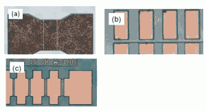
- Figure 1: The optical pictures of ohmic metal surfaces for AlGaN/GaN HEMTs. (a) Ti/Al/Ni/Au with RTA at 800°C; (b) Ti/Al/Ni/Pt with RTA at 950°C; and (c) Ti/Al/Ni/Pt with 20-nm recess and RTA at 950°C.
-
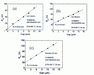
- Figure 2: TLM results of the ohmic contact for AlGaN/GaN HEMTs. (a) Ti/Al/Ni/Au with RTA at 800°C; (b) Ti/Al/Ni/Pt with RTA at 950°C; and (c) Ti/Al/Ni/Pt with 20-nm recess and RTA at 950°.
- H. S. Lee, K. Ryu, M. Sun, and T. Palacios, “Wafer-level heterogeneous integration of GaN HEMTs on Si (100) MOSFETs,” IEEE Electron Device Letters, vol. 33, no. 2, pp. 200-202, Feb. 2012. [↩]
- A. N. Bright, P. J. Thomas, M. Weyland, D. M. Tricker, C. J. Humphreys, and R. Davies, “Correlation of contact resistance with microstructure for Au/Ni/Al/Ti/AlGaN/GaN ohmic contacts using transmission electron microscopy,” Journal of Appl. Phys., vol. 89, no. 6, pp. 3143-3150, Mar. 2001. [↩]