Anisotropic Dry Etching of InGaAs for Self-aligned FETs
- Category: Electronic Devices
- Tags: iii-v materials, jesús del alamo, luke guo
As CMOS technology continues to scale to the nanometer regime, there has been a strong demand for alternative materials to replace silicon. III-V materials, in particular, have shown great promise in extending the road map for high-performance CMOS technology because of their superior electron transport properties [1] . However, many III-V FETs are still fabricated using wet etchants that are difficult to control and give large undercuts, decreasing their feasibility for use in commercial logic applications that require very tight footprints. In addition, oversized gate-source and gate-drain separations result in parasitic series resistances that play a large role in degrading device characteristics. A great need exists for a low-damage and highly anisotropic dry-etch process for scaled logic III-V FETs.
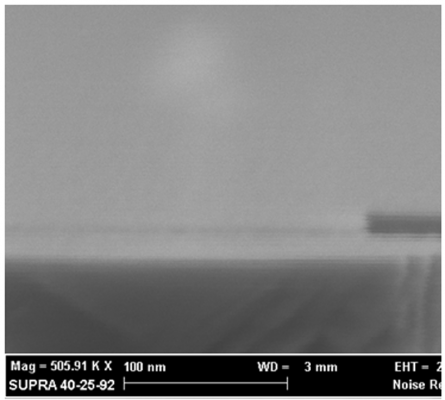
This study explored a dry-etching technique for InGaAs caps using CH4-based chemistry with the addition of SF6. While a CH4/H2 dry etch chemistry gave relatively anisotropic sidewalls with minimal undercut, it was found that this chemistry alone gave rough surfaces, shown in Figure 1. With the addition of SF6 to the discharge, the surface roughness of etched InGaAs was reduced significantly without affecting anisotropy, shown in Figure 2. Furthermore, when the same CH4/H2 dry etch without SF6 was performed on a GaAs surface, it was found to give smooth surfaces, suggesting that the rough surface could be attributed to the formation of indium-based residue
Besides improving the surface roughness of InGaAs dry etching, the addition of SF6 to the CH4/H2 plasma can also promote the use of InAlAs as an etch stop through the formation of AlF3 compounds upon reaching the InAlAs surface [2] . However, a drawback to the use of SF6, and many fluorine-containing compounds, is that it attacks silicon oxide and silicon nitride, reducing the effectiveness of these materials as dry-etching masks.
Our research will continue to explore selective dry etching chemistries for III-V heterostructures that provide smooth, highly anisotropic sidewalls with low damage.
-
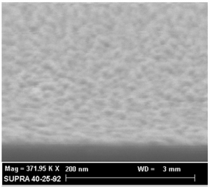
- Figure 1: Surface of an InGaAs sample after a 20-min dry etch using CH4/H2 chemistry with an ECR power of 200W.

-

- Figure 2: The addition of SF6 to the CH4/H2 chemistry appreciably improves the smoothness of etched InGaAs surfaces.