Self-aligned Sub-100-nm InGaAs MOSFETs for Logic Applications
- Category: Electronic Devices
- Tags: dimitri antoniadis, jesús del alamo, mosfets
InGaAs-based metal-oxide-semiconductor field-effect transistors (MOSFETs) have shown great potential for future high- performance and low-power logic applications [1] . Superior electron transport properties [2] and impressive device prototypes have been recently demonstrated [3] [4] . The parasitic resistance is an important problem to address, especially in deeply scaled devices. In addition, the gate-contact separation has to be kept to a minimum to achieve the device footprint goals. We address these requirements by introducing a novel transistor architecture with self-aligned contacts and a gate-last fabrication scheme.
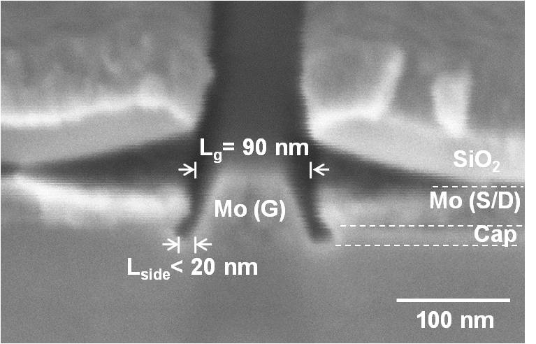
In this work, self-aligned InGaAs quantum-well MOSFETs in the sub-100-nm regime have been demonstrated. A cross- sectional SEM image of a device with gate length of 90 nm is shown in Figure 1. As shown, the S/D metal (Mo) and the n+ cap are self-aligned to the gate. With an optimized recess etch process, the device has achieved a very tight S/D-to-channel spacing (Lside < 20 nm). The channel consists of an InGaAs quantum well buried under a thin InP layer. A composite dielectric consisting of thin layers of Al2O3 and HfO2 is grown by atomic layer deposition (ALD). Well-behaved output characteristics are shown in Figure 2 for a 90-nm-gate length device. The total on-resistance of this device at Vgs-Vt= 0.7 V is 595 W.mm which is an excellent value. The subthreshold swing for a 60-nm-gate device at Vds = 0.5 V is 120 mV/dec. The gate current is below 3×10⁻³ A/cm2 at the maximum operating voltage (Vgs-Vt =0.7 V). The process yields devices with gate lengths down to 30 nm with acceptable parasitic resistance. This self-aligned architecture will enable us to explore the scaling behavior and electron transport characteristics of InGaAs QW-MOSFETs in a dimensional range of interest for future CMOS.
-

- Figure 1: SEM cross-section of a QW-MOSFET with 90-nm gate length and very tight S/D-to gate spacing.
-
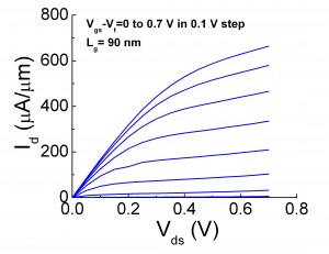
- Figure 2: Output characteristics of a QW-MOSFET with 90-nm gate length.
- J. A. del Alamo, “Nanometer-scale electronics with III-V compound semiconductors,” Nature, vol. 479, pp. 317-323, 2011. [↩]
- D.-H. Kim, B. Brar and J. A. del Alamo, “fT = 688 GHz and fmax = 800 GHz in Lg = 40 nm In0.7Ga0.3As MHEMTs with gm_max > 2.7 mS/μm,” IEDM Tech. Dig., 2011, p. 319. [↩]
- M. Egard, L. Ohlsson, B. M. Borg, F. Lenrick, R. Wallenberg, L.-E. Wernersson, and E. Lind, “High ransconductance self-aligned gate-last surface channel In0.53Ga0.47As MOSFET” in IEDM Tech. Dig., 2011, pp. 304. [↩]
- M. Radosavljevic, B. Chu-Kung, S. Corcoran, G. Dewey, M. K. Hudait, J. M. Fastenau, J. Kavalieros, W. K. Liu, D. Lubyshev, M. Metz, K. Millard, N. Mukherjee, W. Rachmady, U. Shah, and R. Chau, “Advanced high-K gate dielectric for high-performance short-channel In0.7Ga0.3As auantum well field effect transistors on silicon substrate for low power logic applications,” in IEDM Tech. Dig., 2009, pp. 319. [↩]