Nano-scale Contacts for III-V CMOS
- Category: Electronic Devices
- Tags: alex guo, iii-v materials, jesús del alamo
Deeply scaled III-V MOSFETs have demonstrated logic performance at 0.5 V, exceeding that of Si [1] . The gate length of modern III-V MOSFETs has been recently reduced to sub-100-nm dimensions. However, the actual contacts in current research devices still are many times larger than this. Going forward, a key element for a high-performance, small-footprint III-V CMOS technology is the achievement of nanometer-scale source and drain contacts with low contact resistance. This goal is challenging because as the contact length decreases to the nanometer regime, the contact resistance is expected to increase dramatically. This study focuses on characterizing nanometer-scale metal contacts to III-V heterostructures.
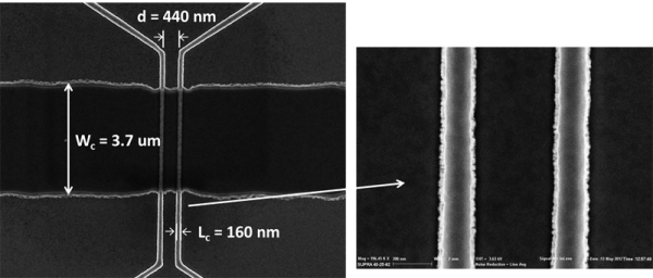
We have first developed a fabrication process to build nano-TLM structures with different contact length (Lc) and spacing (d). We have used Mo contacts to an InGaAs-based heterostructure. Mo definition was achieved by electron-beam lithography followed by dry etching. The mesa and contact pads were formed using photo lithography and a series of dry etching and lift off processes. Figure 1 shows a fabricated nano-TLM structure with ~160-nm contact length and a spacing of ~440 nm. The devices are being characterized using Kelvin (4-terminal) measurements. The sheet resistance of Mo film needs to be considered because the film thickness is decreased to ~50 nm. The contact resistance (Rc) and metal sheet resistance (Rshm) can be extracted using an equivalent circuit model developed for this specific nano-TLM structure. In the future we will expect to integrate nano-scale ohmic contact into a III-V CMOS process, with the goal of reducing transistor footprint and provide insight into the limitations that nano-scale contacts impose on transistor characteristics.

Figure 1: Plan view image of a nano-TLM structure with ~160-nm contact length Mo contacts about ~440 nm apart.
- J. A. del Alamo, “Nanometre-scale electronics with III-V compound semiconductors,” Nature, vol. 479, no. 7373, pp. 317-323, Nov. 2011. [↩]