Graphene Infrared Photodetectors
- Category: Electronic Devices, Materials, Nanotechnology, Optics & Photonics
- Tags: allen hsu, graphene, jing kong, tomas palacios

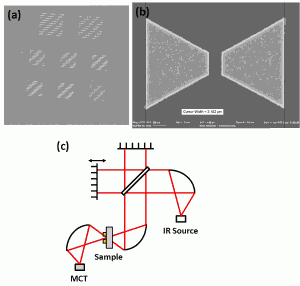
Figure 1: (a) Scanning electron microscopy (SEM) of bowtie array; (b) SEM of single element bowtie; (c) Fourier Transform infrared spectroscopy setup for characterization of graphene infrared photodetectors.
Graphene is a two-dimensional (2D) material that has attracted great interest for electronic devices since its discovery in 2004 [1] . With essentially the same lattice structure as an unwrapped carbon nanotube, graphene shares many of its advantages, such as having the highest intrinsic carrier mobility at room temperature of any known material [2] . This trait, combined with its high electron velocity and thermal conductivity, makes this carbon-based material an excellent candidate for high frequency electronic applications. Furthermore, graphene, due to its zero band gap band structure, also has a broadband optical absorption ranging from the far-infrared (λ>10 µm) all the way to the visible (λ< 532 nm) [3] . Standard state-of-the-art infrared focal plane arrays rely on very exotic materials systems such as InSb and HgCdTe, both of which are difficult to grow as well as difficult to integrate cheaply with silicon read out electronics [4] . Graphene, on the other hand, could enable a new generation of carbon-based infrared photodetectors.
Metal-graphene-metal photodetectors have been demonstrated in the visible range (532 nm) using exfoliated highly oriented pyrolytic graphite (HOPG); however, the external efficiencies of these devices are generally low (<1%) [5] . Graphene photodetectors may intrinsically have efficiencies ranging from 10-15%; however, poor optical coupling with the incident light reduces the overall efficiencies of these devices. Therefore, to better address these issues, we have begun fabrication of large area photodetector arrays utilizing plasmonic antenna elements to better match the incoming light to the spatial response of the graphene photodetectors designed in the infrared (Figure 1 (a) and (b)). Furthermore, using chemically vapor grown graphene, we have been fabricating large array photodetector arrays (1 cm x 1 cm) to better extract power from the incident electromagnetic radiation. The setup for characterizing the optical properties of these photodetectors is shown in Figure 1(c).
- K. S. Novoselov, et al., “Electric field effect in atomically thin carbon films,” Science, vol. 306, pp. 666-669, 2004. [↩]
- Bolotin, et. al., “Ultrahigh electron mobility in suspended graphene,” Solid State Communications, vol. 146, pp. 351-355, 2008. [↩]
- Z. Q. Li, et al., “Dirac charge dynamics in graphene by infrared spectroscopy,” Nature Physics, vol. 4, pp. 532-535, 2008. [↩]
- A. Rogalski, “HgCdTe infrared detector material: History, status, and outlook,” Rep. Prog. Phys, vol. 68, p. 2267, 2005. [↩]
- F. Xia, et al., “Ultrafast graphene photodetector,” Nature Nanotechnology, vol. 4, pp. 839-843, 2009. [↩]