category » Nanotechnology

Lack of technology for high-throughput electronic recordings and simultaneous stimulation is a major limiting factor for the development of neuroprosthetics…
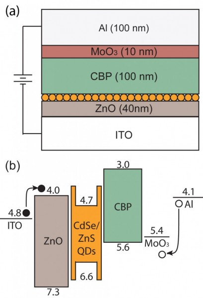
Quantum dot light emitting diodes (QD-LEDs) are promising devices for the next generation of solid-state lighting and other optoelectronic applications….
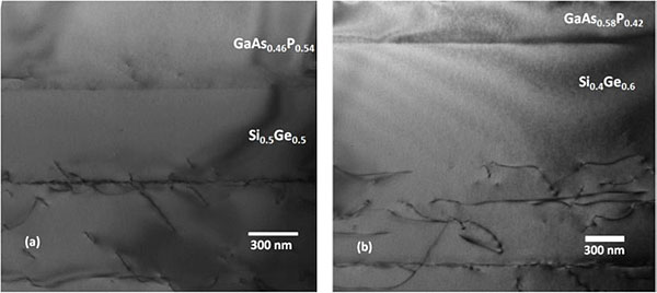
Nitride transistors with current gain cut-off frequencies (fT) of 300 GHz and power gain cut-off frequencies (fmax) of 394 GHz…
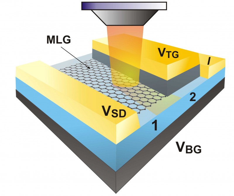
Graphene is a two-dimensional (2D) material that has attracted great interest for electronic devices since its discovery in 2004 [1]…
Catastrophic structural failures cause many physical and personal losses, with prevention estimated at billions of dollars in savings each year….
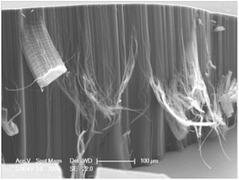
Carbon nanotube (CNT) composites are promising new materials for structural applications thanks to their mechanical and multifunctional properties. We have…
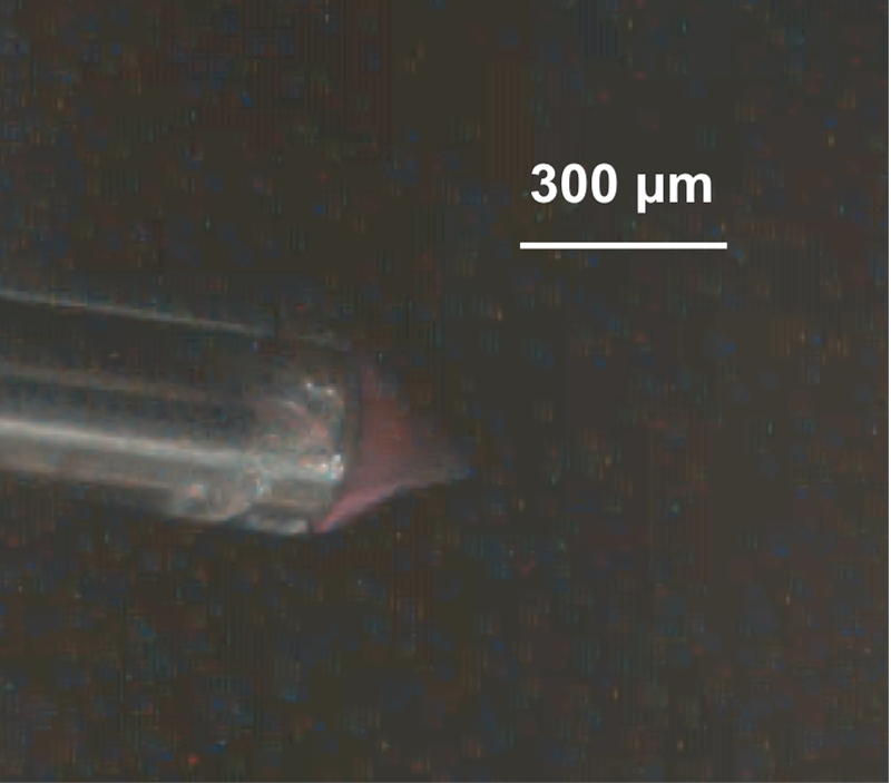
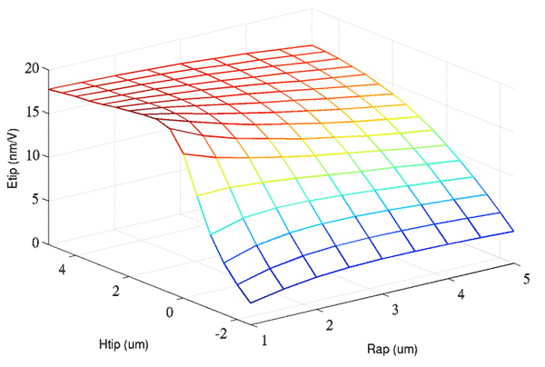
An electrospray emitter ionizes polar liquids using high electrostatic fields. The electric field produces suction on the free surface (meniscus)…
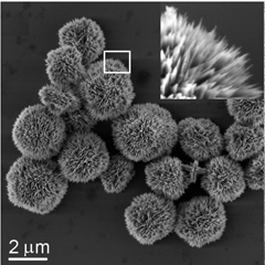
This work focuses on the development of non-metallic substances that can catalyze carbon nanotube (CNT) growth while remaining in a…
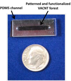
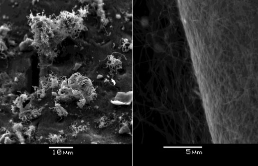
We integrated ultra-porous (99% porous) elements (nanoporous forests of vertically aligned carbon nanotubes (VACNTs)) in MEMS, showing their use in…
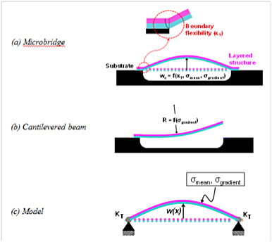
Characterization of thin film layered materials is critical for many MEMS devices. Residual stresses from production determine both final shape…
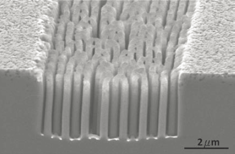
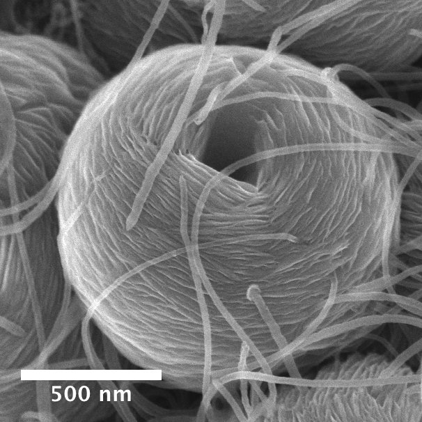
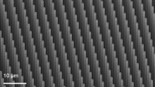
Vertically-aligned carbon nanotube (CNT) arrays are grown on a moving substrate, demonstrating continuous growth of nanoscale materials with long-range order….
Gas sensors are essential in the monitoring, control, and reduction of harmful emissions in the environment [1] . Conductometric gas…
Development of miniature vacuum pumps that can be integrated with electronic or MEMS components is necessary for producing advanced equipment…
Silicon nanowires (NWs) have attracted immense interest for sensing applications due to their high surface-to-volume ratio. In particular, field-effect-based chemical…
Recently, Li-O2 batteries have attracted much attention as potential next-generation alternatives to lithium-ion batteries for electric vehicle energy storage [1]…
Capacitors with high capacitance density (capacitance per footprint area) have potential applications in autonomous microsystems and for power management in…
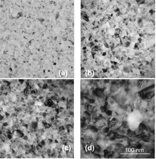
Controlling the intrinsic stress in polycrystalline thin films is of great importance in a wide variety of applications, especially those…
Two-dimensional crystals, including graphene, hexagonal boron nitride, and transition metal dichalcogenides (TMD) materials, have outstanding properties for developing the next…
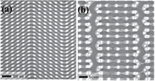
Self-organized macromolecular materials provide an alternative to conventional lithography for fabricating devices on the nanometer scale. Self-assembly of the microdomains…
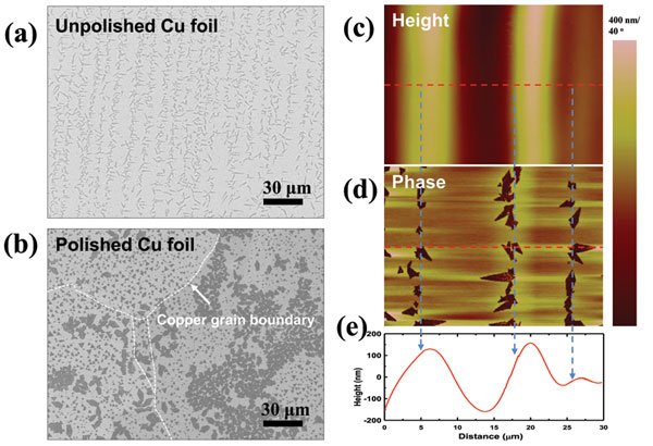
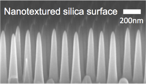
Surfaces play a vital role in heterogeneous crystallization; surface properties such as chemistry, roughness and shape impact nucleation significantly [1]…
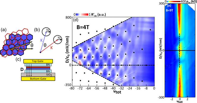
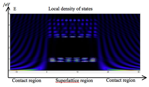
The bilayer 2-dimensional electron gas (2DEG) consists of two closely spaced 2DEGs, between which Coulomb interactions and tunneling effects can…
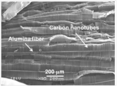
Due to their mechanical, thermal, and electrical properties and their natural ability to grow on a variety of metallic and…
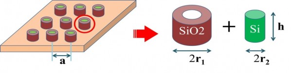
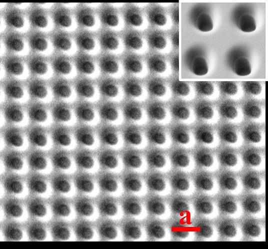
Solar cells with broadband absorption and large acceptance angle are demonstrated by using two-dimensional core-shell structures, which are composed of…
Two-dimensional photonic crystals (PhCs) are fabricated using dual-beam focused ion beam (FIB) in Er3+-TeO2 thin films and demonstrate broadband enhancement…
Hexagonal boron nitride (h-BN) is very attractive for many applications, particularly as a protective coating, dielectric layer/substrate, transparent membrane, or…
Due to the remarkable physical properties of graphene, applications in various areas such as transistors [1] , chemical sensors [2]…
The photoresponse of semiconductors, which determines the performance of optoelectronic devices, is governed by energy relaxation pathways of photoexcited electron-hole…
Nanowires are an exciting architecture for light emitting diodes (LEDs). To address the challenges of solid state lighting, III-V nitride…
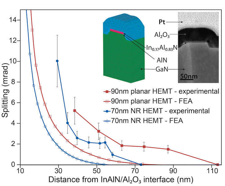
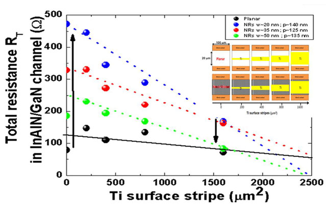
GaN-based high electron mobility transistors (HEMTs) are an important platform for the realization of high-power, high-frequency devices. Nanoribbon (NR) HEMT…
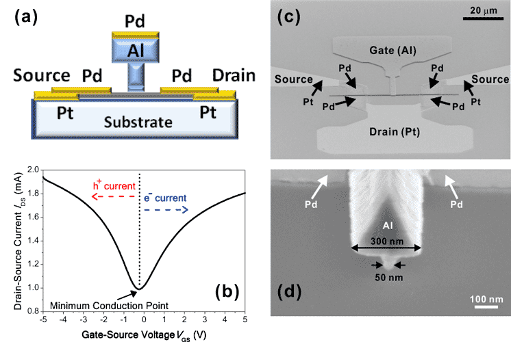
Achieving a sharp subthreshold swing is crucial to enable the supply voltage scaling that is necessary to reducing power consumption…
Photovoltaics and sustainability have received much attention lately. We seek a tandem photovoltaic device using silicon as both the substrate…
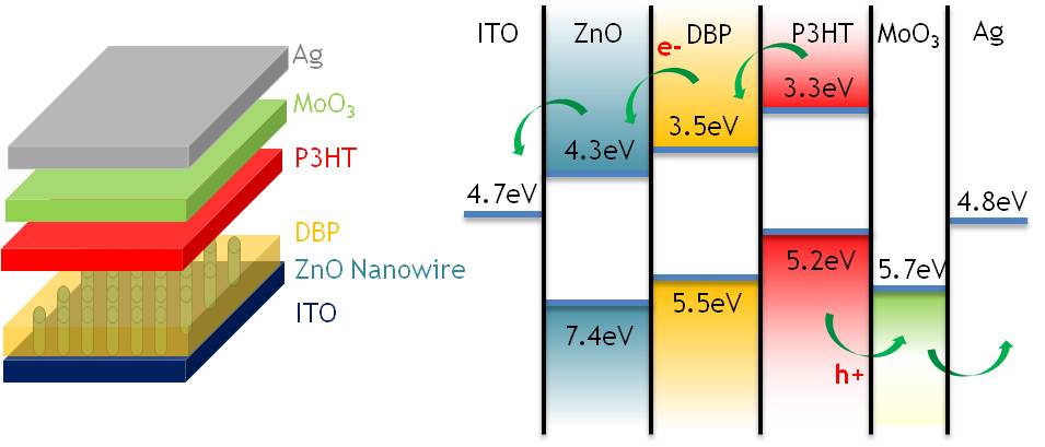
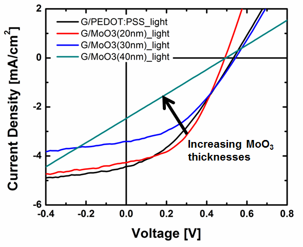
Organic/inorganic hybrid solar cells based on the integration of conductive polymers into semiconducting nanowire arrays offer opportunities for the development…
Microfabricated cantilever beams are used in microelectromechanical systems (MEMS) for a variety of sensor and actuator applications. Bimaterial cantilevers accurately…
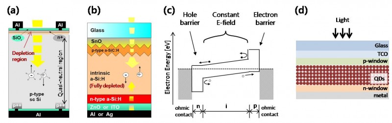
Nanostructured solar cells are attracting increasing attention as a promising photovoltaic (PV) technology [1] . Generation of free charge carriers…
Solar cells based on lead sulfide quantum dots (PbS QDs) represent a promising new class of solution-processable photovoltaics. The highly…
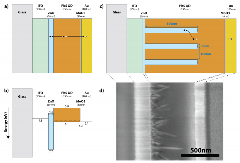
Thin-film solar cells incorporating colloidal quantum dot active layers have recently emerged as a notable third-generation photovoltaic (PV) technology, largely…
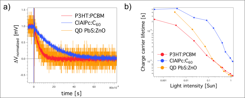
Disordered semiconductors exhibit poor electronic transport properties due to their amorphous nature. Low carrier mobility and lifetime limits the diffusion…
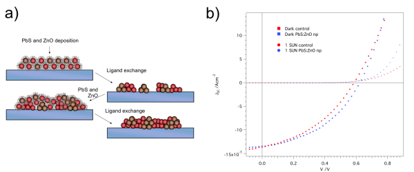
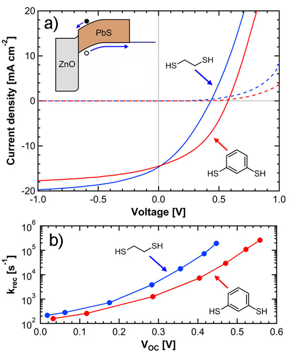
Colloidal lead sulfide quantum dot (PbS QD) solar cells have recently shown attractive improvements in efficiency [1]. PbS QDs have…
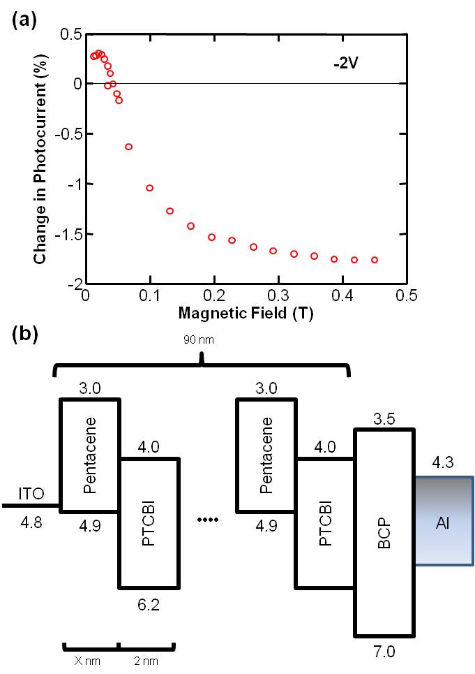
Organic solar cells and photodetectors that feature singlet exciton fission materials have two additional exciton processes that traditional organic solar…
Natural biological surfaces have evolved to optimize their physicochemical properties and structures at the micro/nanoscale for a wide variety of…
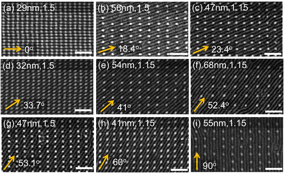
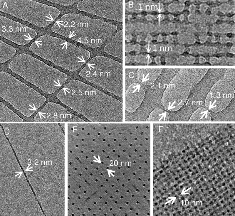
Topographic templates can be used for guiding the self-assembly of block copolymers to produce complex nanoscale patterns. In our previous…
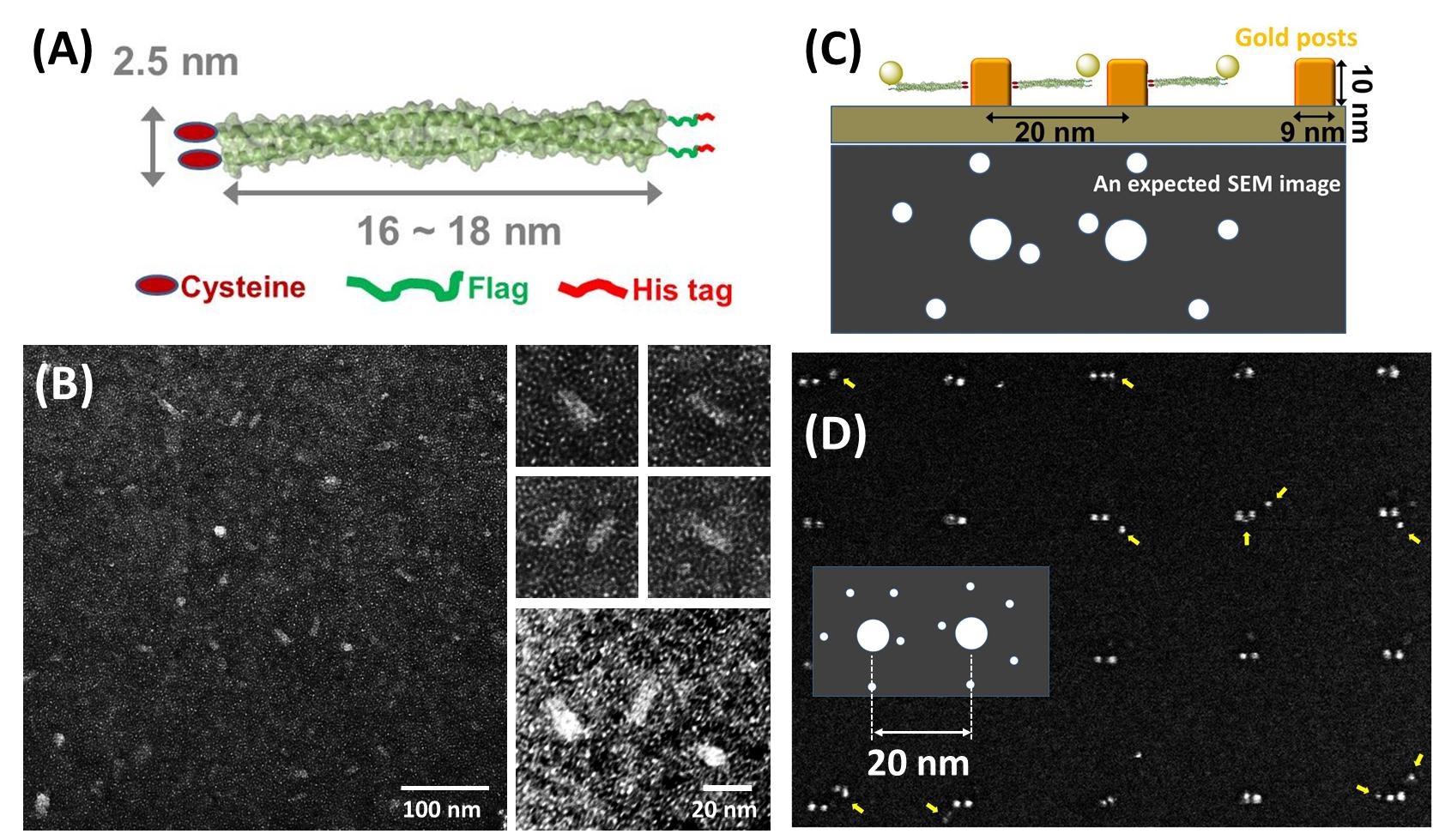
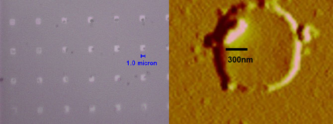
Templated assembly of biomolecules can create complex nanostructured devices with precisely tailored chemical or biological responses, with applications in, for…
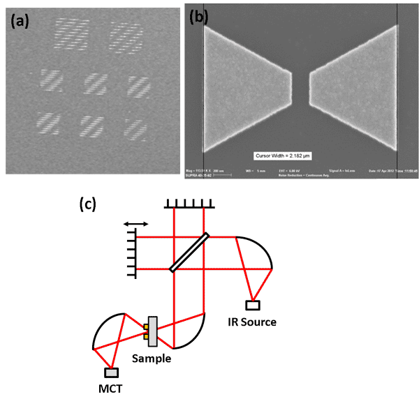
Electron-beam lithography (EBL) readily enables the fabrication of sub-10-nm features [1] . However, the resolution limits of this technique at…
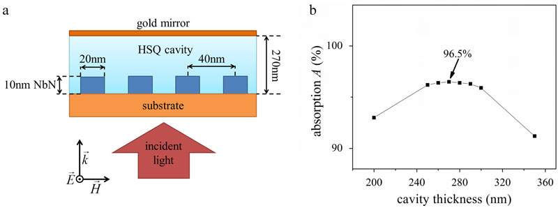
Superconducting nanowire single-photon detectors (SNSPDs) [1] , based on 100-nm-wide, ~ 4-nm‑thick niobium nitride (NbN) nanowires, are unmatched in sensitivity [2]…
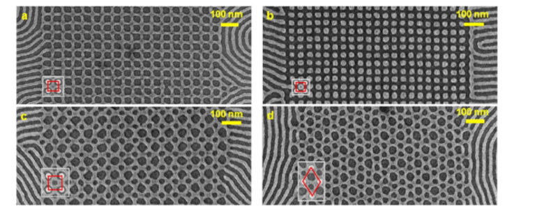
Self-assembled block copolymer structures are useful in nanolithography applications, producing patterns with high resolution and throughput. We previously showed control…
The system detection efficiency of systems integrated with superconducting nanowire single photon detectors (SNSPDs) has been limited to 24% due…
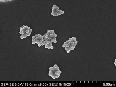
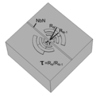
Previously we proposed a particle agglomeration model for chemical mechanical planarization (CMP) with the primary motivation of understanding the creation…
A collaboration of RLE and MTL investigators is creating the scientific and engineering knowledge for a compact coherent X-ray source…
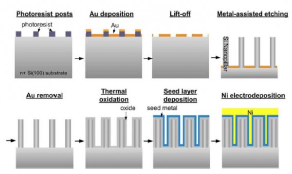
Field emission arrays (FEAs) are an attractive alternative to mainstream thermionic cathodes, which are power hungry and require high vacuum…