Impact of Metal-induced Strain in InAlN/GaN Nanoribbons
- Category: Nanotechnology
- Tags: gallium nitride, mohamed azize, omar saadat, tomas palacios
Nitride transistors with current gain cut-off frequencies (fT) of 300 GHz and power gain cut-off frequencies (fmax) of 394 GHz have been reported [1] [2] . However, the frequency performance of these devices is still far from the theoretical limit due to poor gate modulation efficiency, short channel effects, high access resistances (Ra), and specific contact resistance (rc). Nanoribbon (NR)-based nitride HEMTs could overcome many of these limitations by improving the electron confinement thanks to the excellent electrostatics of wrap-around gates [3] . Moreover, strong piezoelectric-induced doping can be generated in NR nitride-based semiconductors and increase the maximum operating frequency of nitride devices by reducing the parasitic resistances (Ra and rc). In this project, we study the use of Ti-induced strain in InAlN/GaN NR HEMTs.
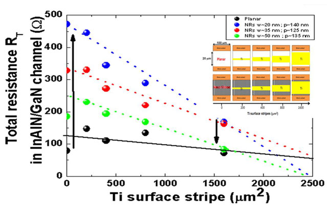
NR and planar devices are fabricated on the same chip. A Ti/Al/Ni/Au metal stack is then deposited for ohmic contact formation. Electron beam lithography and dry etching are performed in some devices to define NR structures between the ohmic contacts with widths (w) in the w~20-90 ± 10 nm range and a period (p) of p~135 ± 10 nm. An additional Ti strip was deposited between the ohmic contacts (cf. inset of Figure 2) with a width of ~100 mm and a length varying from ~2 to 16 mm and annealed at 870 ◦C for 30 s in N2 environment. Figure 1 shows the total resistance RT in NR and planar devicesas a function of the area coverage of the Ti stripes. A quasi-linear RT decrease is observed when the Ti surface area increases in the InAlN/GaN NRs samples, unlike in the planar device. The mechanical stress introduced by Ti stripes has a strong effect on the transport properties of InAlN/GaN NRs. Figure 2 shows the decrease of the sheet resistance (RshTi) underneath the Ti stripe in InAlN/GaN NRs as a function of NR widths. The RshTi in the NR and planar devices is decreased by ~50-75 % and ~10%, respectively.
-
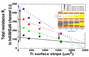
- Figure 1: Total resistance in InAlN/GaN channel as a function of the area coverage of the Ti stripes. The inset shows a cartoon of NR and planar devices with different area coverage of the Ti stripes.
-
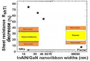
- Figure 2: Sheet resistance underneath of the Ti metal stripes in InAlN/GaN devices as a function of the NR width. The inset shows a cartoon of NR and planar devices with identical area coverage of the Ti stripes.

- D. S. Lee, X. Gao, S. Guo, D. Kopp, P. Fay, and T. Palacios, “300-GHz InAlN/GaN HEMTs with InGaN back barrier, IEEE Electron Device Lett., to be published. [↩]
- K. Shinohara, D. Regan, I. Milosavljevic, A. L. Corrion, D. F. Brown, P. J. Willadsen, C. Butler, A. Schmitz, S. Kim, V. Lee, A. Ohoka, P. M. Asbeck, and M. Micovic, “Electron velocity enhancement in laterally scaled GaN DH-HEMTs with fT of 260 GHz,” IEEE Electron Device Lett., vol. 32, no. 8, pp. 1074-10176, Aug. 2011. [↩]
- W. Lu, P. Xie, and C. M. Lieber, “Nanowire transistor performance,” IEEE Trans. Electron Dev., vol. 55, no 11, pp 2859-2876, Nov. 2008. [↩]