Cavity-integrated Ultra-narrow Superconducting Nanowire Single-photon Detector Based on a Thick Niobium Nitride Film
- Category: Nanotechnology, Optics & Photonics
- Tags: faraz najafi, karl berggren, niobium
Superconducting nanowire single-photon detectors (SNSPDs) [1] , based on 100-nm-wide, ~ 4-nm‑thick niobium nitride (NbN) nanowires, are unmatched in sensitivity [2] and timing accuracy [3] by other detector technologies at standard optical telecommunication wavelengths. The detection efficiency (η) of SNSPDs is the product of the optical absorption of the nanowire meander (A, which increases with the thickness of the nanowires) and the probability of photon induced resistive state formation in the nanowire (Pr, which increases with decreasing cross-sectional area of the nanowires [4] ).

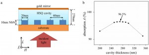
Figure 1: (a) Cross-sectional view of an SNSPD based on 20-nm-wide and 10-nm-thick NbN nanowires with an integrated HSQ cavity. The pitch is 40 nm (the nanowires fill 50% of the detector area). The detector is illuminated from the back of the substrate with light polarized in parallel to the nanowires. The thickness of the cavity was optimized for maximum absorption in the NbN nanowires. The optimum cavity thickness was found to be 270 nm. (b) Simulated optical absorption at 1550-nm wavelength for the geometry shown in (a) as a function of cavity thickness.
We propose a high‑detection‑efficiency detector based on ultra-narrow (20-nm‑wide), thick (10‑nm‑thick instead of 4-nm-thick) nanowires arranged in a 50%-fill-factor meander. In this detector, we expect the decrease of Pr due to the thicker nanowire to be compensated by reducing the width of the nanowire down to 20 nm. When integrated with a quarter-wavelength optical cavity, as shown in Figure 1a, this detector is expected to have a peak optical absorption of 96.5% (Figure 1b, based on a COMSOL model reported in Ref. [5] ). The nanowire cross-sectional area (200nm2) of the proposed detector is comparable to the nanowire cross-sectional area of ultranarrow-nanowire SNSPDs (~ 150nm2, as in Ref. [6] ), which have Pr ~ 0.9. If we assume the same Pr value for the proposed detector, it is expected to have a detection efficiency of η = Pr * A ~ 87%. A 15% variation in the cavity thickness is expected to result in a variation of < 1% in the absorption, further relaxing the fabrication constraints. We are currently working on the experimental implementation of this cavity-integrated detector.
- G. N. Gol’tsman et al., Applied Physics Letters vol. 79, p. 705, 2001. [↩]
- A. Korneev et al., IEEE T Appl Supercon vol. 15, pp. 571-574, 2005. [↩]
- E. A. Dauler et al., IEEE T Appl Supercon, vol. 17, pp. 1051-8223, 2007. [↩]
- A. Semenov et al., The European Physical Journal B, vol. 47, pp. 495-501, 2005. [↩]
- V. Anant et al., Opt Express vol. 16, pp. 10750-10761 (2008) [↩]
- F. Marsili et al., Nano Letters vol. 11, p. 2048, 2011. [↩]