Evolution of Intrinsic Stress and Grain Structure in Polycrystalline Films for Nano/Micro-electromechanical System Applications
- Category: MEMS & BioMEMS, Nanotechnology
- Tags: carl thompson, hang yu, wubin bai
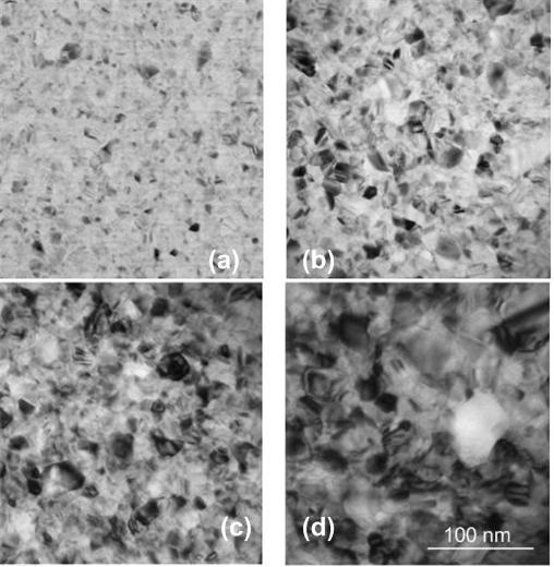
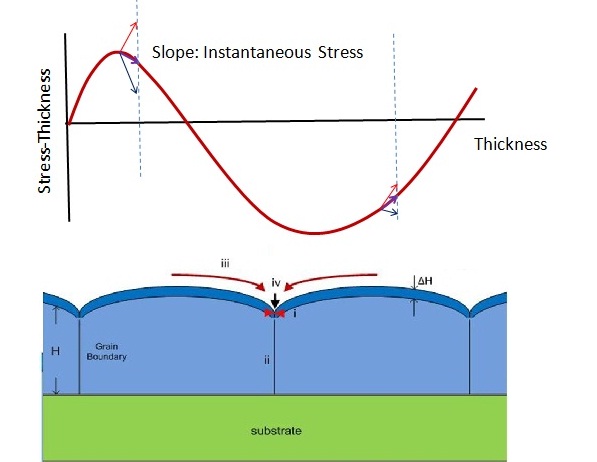
Controlling the intrinsic stress in polycrystalline thin films is of great importance in a wide variety of applications, especially those in which mechanical properties and reliability issues are critical, e.g., Nano-/microelectromechanical systems (N/MEMS). Using capacitance techniques, intrinsic stress can be monitored in situ and in real time during deposition processes. We do this in a UHV e-beam evaporator in which we grow FCC metal films at a range of homologous temperatures, in a range of deposition rates, and with variable vacuum conditions. These studies show an evolution to a high tensile stress during film formation (Type I behavior), or an evolution first to a tensile stress and then to a compressive stress at higher thicknesses (Type II behavior). The origin of this behavior, especially Type II behavior, is not well understood. In recent studies we have found that Pd and Ni deposited at intermediate homologous temperatures undergo a behavior intermediate to that of Type I and Type II (Figure 1), where the stress evolves from tensile to compressive and back to tensile. Transmission electron microscopy (TEM) reveals that the grain size increases during deposition at low or intermediate homologous temperatures. The grain size in Ni films deposited from 300K to 473K forms a linear relation with film thickness. Figure 2 shows representative bright field TEM images of Ni films deposited at 473K. It is known that grain growth in a constrained film leads to tensile stress. We believe that while the first tensile rise is associated with a coalescence stress, the second is associated with grain growth. Grain growth itself leads to a tensile stress and also to a lower rate at which ad-atom are trapped at boundaries to cause compressive stresses. We find that changes in the deposition conditions can modify this behavior.
-
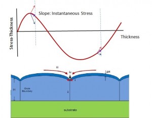
- Figure 1: Upper: Stress evolution at intermediate homologous temperatures. Both compressive and tensile components are involved. Lower: Schematic of processes during film growth. i: GB closure, ii: grain growth, iii and iv: adatom trapping at boundaries.
-

- Figure 2: Bright field TEM images of Ni films deposited at 0.5Å/s, with the substrate temperature kept at 473K.The film thicknesses of (a) to (d) are 7, 20, 37, and 55 nm, respectively.