Silicon Nanowires for Chemical Sensing Systems
- Category: Energy, Nanotechnology
- Tags: ahmed al-obeidi, carl thompson
Silicon nanowires (NWs) have attracted immense interest for sensing applications due to their high surface-to-volume ratio. In particular, field-effect-based chemical sensors are an attractive platform for fabricating multi-channel analysis systems capable of detecting bio-molecule concentrations and enzyme reactions. One can measure the concentrations of target analytes by taking advantage of changes in either capacitance or conductivity due to binding of chemical and biological species to the NW surface. However, most nanowire-based biochemical sensor studies employ planar field-effect transistor (FET) structures. In comparison, vertical freestanding FET structures sensors have a greater potential for ultrahigh sensitive detection because of the still larger exposed surface interaction area in high density arrays.
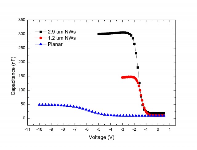
One solution to fabricating vertically aligned FETs is through metal-catalyzed etching (MCE) [1] [2] , a low-cost, room temperature method which enables fabrication of highly ordered Si NW arrays of large aspect ratios (Figure 1). Such structures are very promising for the detection of multiple targets in an integrated microfluidic system. Improvement in sensor sensitivity using an electrolyte-semiconductor-silicon (EIS) sensor system was found to scale with nanowire length, translating into a stronger sensor signal when compared to a planar EIS sensor (Figure 2).
-
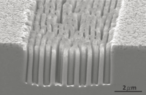
- Figure 1: Vertical silicon nanowire arrays in channels using metal- catalyzed etching.

-
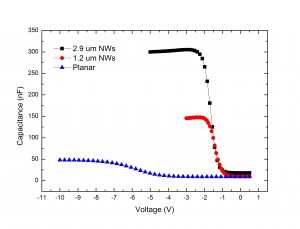
- Figure 2: C/V curves for planar and NW-based EIS sensors. Enhancement in capacitance, or effective sensors signal, scales with increasing surface area. Signal enhancement was 3 times and 6 times that of the planar system for the short and long nanowire systems, respectively.
- S. W. Chang, V. P. Chuang, S. T. Boles, C. A. Ross, and C. V. Thompson, “Densely packed arrays of ultra‐high‐aspect‐ratio silicon nanowires fabricated using block‐copolymer lithography and metal‐assisted etching,” Advanced Functional Materials, vol. 19, pp. 2495-2500, Aug. 2009. [↩]
- S. W. Chang, V. P. Chuang, S. T. Boles, and C. V. Thompson, “Metal‐catalyzed etching of vertically aligned polysilicon and amorphous silicon nanowire arrays by etching direction confinement,” Advanced Functional Materials, vol. 20, pp. 4364-4370, Dec. 2010. [↩]