Photonic Crystals on Erbium-doped Tellurite Thin Films for Broadband-enhanced Photoluminescence at near Infrared
- Category: Energy, Materials, Nanotechnology, Optics & Photonics
- Tags: lionel kimerling, pao lin
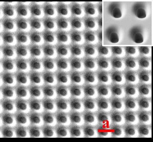
Two-dimensional photonic crystals (PhCs) are fabricated using dual-beam focused ion beam (FIB) in Er3+-TeO2 thin films and demonstrate broadband enhancement of PL emission at near Infrared (NIR). As Figure 1 shows, highly uniformed patterns with smooth surfaces and pattern resolution better than hundred nanometers are achieved. PhCs arrays with photonic lattice constants ranging from 350 nm to 1700 nm are explored to optimize the PL extraction efficiency. Strong photoluminescence around 1530 nm is observed using 488-532 nm laser pump. A confocal microscope with spectrometer is used to capture the broadband PL signals from individual PhC arrays.
The emission enhancement factor and spectral dependent extraction ratio were analyzed to find the interaction between PL emission and PhC structures. Figure 2 (a) shows that when the PhC structures are optimized, 1500 µm-1560 µm broadband PL is successfully converted between the PL in-plane and out-of-plane emission. As in Figure 2(b), a 60 % enhancement of surface extraction efficiency is achieved when PhC with periodicity a=800 nm is applied. When photonic lattice constants a are smaller than the critical periodicity of 600 nm, the PL light becomes confined inside the thin film layer. Two-dimensional finite difference time domain (FDTD) simulation explains the experimentally observed anisotropic PL enhancement as due to the photonic band gap. The broadband PL enhancement enables Er3+-TeO2 PhCs thin film as a potential light source for three- dimensional integrated photonic circuits.
-
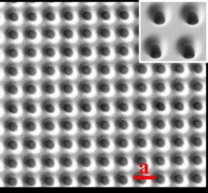
- Figure 1: SEM surface image of the patterned Er3+-TeO2 thin film PhCs. The insert (upper right) is a cross-sectional image captured at a tilt angle of 36o. Photonic lattice constant a=700 nm is labeled by the red bar.
-
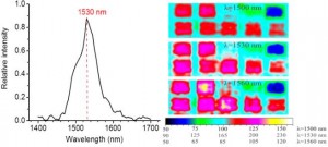
- Figure 2: (a) PL spectrum obtained when the Er3+-TeO2 thin film is excited by a 532-nm laser. (b) PL mapping at λ=1500 nm, 1530 nm and 1560 nm. The periodicities of the 2 x 5 PhC array starting from the top right going counterclockwise are 360 nm, 490 nm, 630 nm, 800 nm, 950 nm, 1050 nm, 1180 nm, 1330 nm, 1430 nm, and 1670 nm, respectively. Below the PL mapping is the scale bar at different λ.

- P. T. Lin, M. Vanhoutte, N. S. Patel, V. Singh, J. Hu, Y. Cai, R. Camacho-Aguilera, J. Michel, L. C. Kimerling, and Anu Agarwal, “Engineering broadband and anisotropic photoluminescence emission from rare earth doped tellurite thin film photonic crystals,” Optics Express, vol. 20, no. 3, pp. 2124-2135, 2012.