An Analytical Approach for Characterizing the Complete Stress State in Thin-film CMOS Layered Materials and 3D MEMS Design via Postbuckling
- Category: MEMS & BioMEMS, Nanotechnology
- Tags: brian wardle, fabio fachim
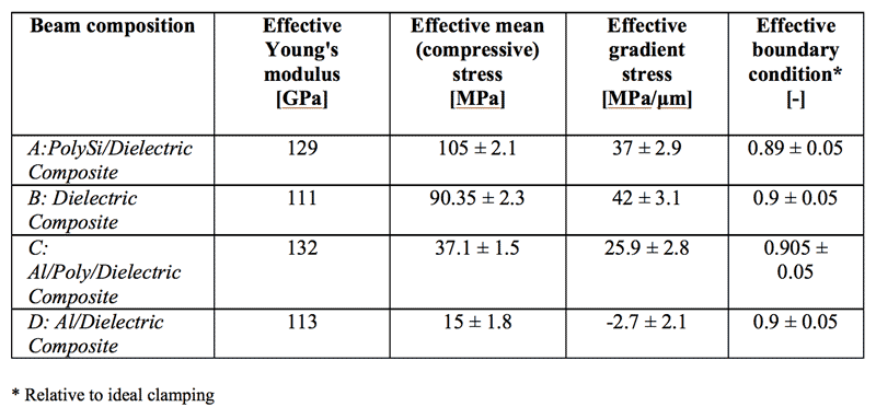
Characterization of thin film layered materials is critical for many MEMS devices. Residual stresses from production determine both final shape and performance of microdevices and should therefore be accurately determined. Stresses are typically extracted using simple test structures (clamped beams and cantilevers, see Figures 1a-b) that allow for mean and gradient residual stress estimation [1]. However, current approaches to material characterization have two major limitations. First, their accuracy is directly proportional to their cost. This is especially true for mean compressive stress, where more accurate estimates require a larger number of different test structures. Second, they oversimplify test-structure boundary conditions by considering them to be ideal (e.g., perfectly clamped in the case of buckled beams for mean compressive stress determination [1] ). To overcome these issues, we have developed a new methodology for characterizing the complete stress state (effective mean and gradient stresses) in CMOS layered materials that also assesses non-ideality of clamped boundaries [2] [3] . The approach uses a closed-form solution of the postbuckling problem of micromachined beams including non-ideal boundaries (Figure 1). In Table 1 we show the results relative to the characterization of four different CMOS material combinations. The outcomes show mean compressive stresses ranging between -15 and -105MPa, thus demonstrating the method’s ability to characterize structures subjected to both large and small compressive stresses. This ability contrasts with traditional critical length methods that encounter difficulties in quantifying small compressive stresses due to their inability to distinguish between mean stress and gradient stress effects [2] . For the CMOS materials examined here, the accuracy was ± 2MPa for mean stresses and ±3MPa/µm for gradients. Boundary non-ideality is found to be 90% of perfectly clamped for the CMOS-released films, having such a significant effect on the extracted stresses that it must be considered. The analytical tool can also be extended to 3D MEMS design, where buckling is used to controllably place structural elements outside the wafer plane. Using this approach, we have demonstrated out-of-place architectures for applications from three-axis thermal sensing to 3D flow measurement [4] ).
-
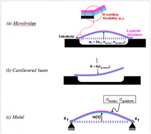
- Figure 1: Post-release out-of-plane deformation of micromachined structures [2] .
-
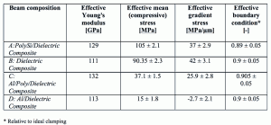
- Table 1: Characterization of thin film CMOS layered materials using analytical models [2]
- M. J. Madou, Fundamentals of Microfabrication: The Science of Miniaturization, 2nd Edition, New York: CRC Press, 2002. [↩]
- F. Fachin, M. Varghese, S. A. Nikles, and B. L. Wardle, “Characterization of the complete stress state in thin-film CMOS layered materials,” in Proc. Hilton Head, 2010. [↩] [↩] [↩] [↩]
- F. Fachin, S.A. Nikles, J. Dugundji, and B. L. Wardle, “Analytical extraction of residual stresses and gradients in MEMS structures with application to CMOS-layered materials,” Journal of Micromechanics and Microengineering, vol. 21, pp. 095017095025 , 2011. [↩]
- F. Fachin, S. A. Nikles, and B. L. Wardle, “Mechanics of out-of-plane MEMS via post-buckling: Model-experiment demonstration using CMOS,” Journal of Microelectromechanical Systems, to be published. (Available in Early Access Form at http://ieeexplore.ieee.org [↩]