Photoactuated Ultrafast Silicon Nanostructured Electron Sources for Coherent X-ray Generation
- Category: Nanotechnology
- Tags: karl berggren, luis velasquez-garcia, michael swanwick
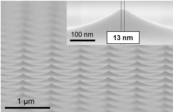
A collaboration of RLE and MTL investigators is creating the scientific and engineering knowledge for a compact coherent X-ray source for phase contrast medical imaging based on inverse Compton scattering of relativistic electron bunches. The X-ray system requires a low emittance electron source that can be switched at timescales of tens of femtoseconds or faster; the focus of our work has been the design, fabrication and characterization of massive arrays of a nanostructured high aspect-ratio silicon (Si) structures to implement low-emittance and high-brightness cathodes that can be triggered very fast using laser pulses to produce spatially uniform electron bunches. Si nanostructure arrays with highly uniform sub-10 nm tip radii have been fabricated via a combined optical lithography and diffusion limited oxidation technique. The fabrication process allows nanometer-level control over the dimensions of the electron emitter structures. Figure 1 shows an array of Si tips with 1.25 µm hexagonal pitch have an average radius of curvature of 6.2 nm and standard deviation of 1.1 nm (n=29); when the radius of curvature is changed to 21.6nm, the standard deviation remains approximately the same, i.e., 1.25 nm (n=69).
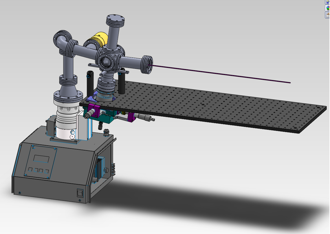
The tips are illuminated at a grazing incidence of roughly 84 degrees with a 1 kHz titanium sapphire laser (800 nm wavelength) with a pulse duration of 35 fs; the high electric field of the laser pulse is amplified by the silicon tips so the electrons can quantum tunnel from the tips into the vacuum. Experimental results using a time of flight spectrometer show electron beamlet array emission with 3-photon absorption. Work is ongoing to optimize the tip geometry for both low emittance and high current. We are also designing and building a new vacuum chamber to test the devices (Figure 2). The chamber will pump down to 10-7 torr in ~15min with an anode bias up to 1100V.
-
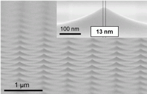
- Figure 1: A SEM micrography of highly uniform nanosharp tips with 1.25 µm hexagonal pitch and 12.4 nm average diameter. Upper Right – Close up of a single tip.
-
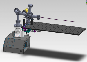
- Figure 2: CAD drawing of new vacuum chamber to measure current from the photo-cathodes using a 35 fs 800nm beam at 1kHz at 84 degree angle.