Recess Integration of Vertical-cavity Surface-emitting Laser Pills and Edge-emitting Laser Platelets on Si
- Category: Medical Electronics, Optics & Photonics
- Tags: clifton fonstad
Optoelectronic devices intimately integrated on silicon integrated circuits have long been sought for optical intercon-nect applications, optical communications modules, and–more recently–neural stimulation and sensing. Toward this end we have recently demonstrated a new heterogeneous integration technique for integrating vertical cavity surface emitting lasers (VCSELs) and edge-emitting laser diodes (EELs) on silicon CMOS integrated circuits [1] [2] .
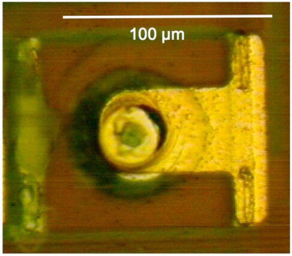
Fully processed and tested oxide-aperture VCSELs emitting at 850 nm have been fabricated as individual “pills” 55 µm in diameter and 8 µm tall with a disk contact on the n-type backside and a ring contact on the p-type, emitting top-side. Similarly, 1.55-µm emitting micro-cleaved cavity EEL platelets 5 µm thick, 150 µm wide, and 300 µm long have also been fabricated. Using a custom micro-pipette vacuum pick-up tool, these micro-laser pills and platelets have been placed on contact pads at the bottom of recesses etched though the dielectric over coating on a Si chip, and batch solder-bonded in place using a custom pressurized-diaphragm bonding apparatus. Back-end processing of the chip then continues with surface planarization, contact via formation, and interconnect metal deposition and patterning. An example of a completely integrated VCSEL pill appears in Figure 1.
No adverse effects are seen from fabricating laser diodes as freestanding pills and platelets. Devices integrated in this manner show the same high performance as devices left on their native substrates and in fact have superior thermal characteristics, largely due to the better thermal conductivity of Si over that of GaAs and InP.
The technique demonstrated in this work offers numerous other advantages over alternative heterogeneous integration techniques. Both the devices to be integrated, and the target circuit wafers, are fabricated under optimal conditions and are pre-tested and screened prior to integration to insure high yield. Significantly, many different types of devices can be integrated on the same IC wafer, a feature unique to this approach. Furthermore, the integration process effectively avoids thermal expansion mismatch limitations and wafer diameter mismatch issues, and it is compatible with parallel assembly techniques, such as fluidic self-assembly.
-
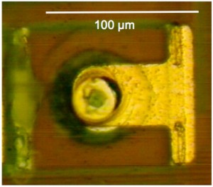
- Figure 1: A microphotograph of a fully integrated VCSEL in its recess on a CMOS chip showing the upper contact pattern connecting the VSCEL to the underlying circuitry. The emission comes from the small aperture in the contact pattern roughly in the center of the picture. The threshold current for integrated pill VCSELs like this is typically 2 mA or less.
-
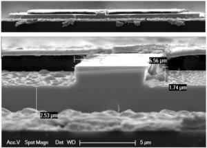
- Figure 2: Close-up photomicrographs showing, in the top portion of the figure, a platelet bonded on a silicon wafer. A close-up view of the micro-cleaved end facet and the ridge waveguide is shown in the lower portion of the figure. Note also the stripe ohmic contact on top of the mesa and the broad-area top contact pad (insulated by a BCB support layer).

- J. M. Perkins, and C. G. Fonstad, “ Full recess integration of small diameter low threshold VCSELs within Si-CMOS ICs,” Optics Express, vol. 16, no. 18 pp. 13955-13960, 2008. [↩]
- J. J. Rumpler and C. G. Fonstad, Jr., “Continuous-wave electrically pumped 1.55 µm edge-emitting platelet ridge laser diodes on silicon,” IEEE Photonics Technology Letters, vol. 21, pp. 827-829, 2009. [↩]