Thin-Film Crystalline Silicon Solar Cells Enabled by Sub-micrometer Surface Light-Trapping Structures
- Category: Energy, Optics & Photonics
- Tags: gang chen, matthew branham
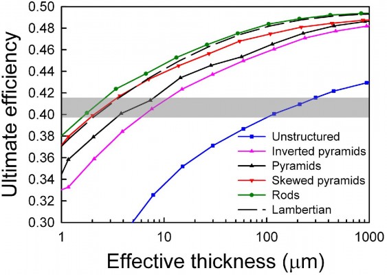
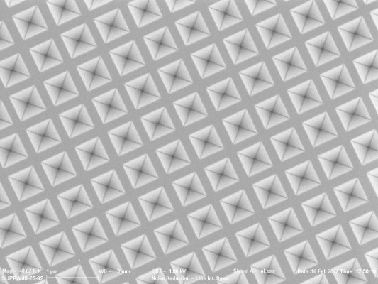
The cost of silicon solar cells has fallen precipitously in recent years, primarily as a result of manufacturing improvements, increasing scale, and decreasing profit margin. Further cost reductions will depend upon technical advances that increase cell efficiency and/or minimize the variable costs associated with module production. One strategy to lower the cost of silicon photovoltaic modules is to dramatically reduce the amount of material required in a cell from the current 180-μm standard to 10 μm or less. However, since the absorption length for longer-wavelength photons (red and infrared) is significantly larger than this thickness, thin cells must be designed to trap photons in the absorber layer very effectively to yield competitive efficiencies. Light-trapping in conventional wafer-based photovoltaics is well understood [1] , and light-trapping structures are integrated into virtually all commercially available solar cells. However, the physical basis associated with light-trapping in thin-film silicon cells is quite different than that for conventional silicon photovoltaics, both because the thinness of the material physically limits the dimensions of light-trapping features and because light-trapping based on geometric optics is less effective for very thin materials. In this work, simulations based on the transfer matrix method were developed to identify optimal surface structures for light trapping. As shown in Figure 1, a variety of potential geometries offer significant enhancement over a planar silicon surface. Of the structures that are modeled in this work, the one offering the best combination of light-trapping effectiveness and manufacturability is a two-dimensional periodic array of inverted pyramids on a sub-micrometer pitch [2] [3] , as in Figure 2. Theoretical calculations suggest that a 10 μm silicon film textured in this way can absorb as effectively as a flat film 300 μm thick. Demonstration versions on SOI substrates are currently being fabricated in the Microsystems Technology Laboratories at MIT.
-

- Figure 1: Solar cell ultimate efficiency as a function of active layer thickness for silicon with various surface textures [3].
-
- Figure 2: SEM image of two-dimensional array of inverted pyramids formed in silicon using projection lithography, 40.6 kX magnification.
- P. Campbell and M. A. Green, “Light-trapping of pyramidally textured surfaces,” Journal of Applied Physics, vol. 62, no. 1, pp. 243-249, July 1987. [↩]
- S. E. Han and G. Chen, “Toward the Lambertian limit of light-trapping in thin nanostructured silicon solar cells,” Nano Letters, vol. 10, pp. 4692-4696, Oct. 2010. [↩]
- S. E. Han, A. Mavrokefalos, M. S. Branham, and G. Chen, “Efficient light-trapping nanostructures in thin silicon solar cells,” Proc. of SPIE: Micro- and Nanotechnology Sensors, Systems, and Applications III, 2011, vol. 8031, p. 80310T. [↩]