Adiabatic Resonant Microring (ARM) Modulator
- Category: Optics & Photonics
- Tags: michael watts
High-performance devices and systems based on CMOS-compatible silicon photonics are increasingly gaining momentum in the optical interconnects community as essential building blocks for high-speed, energy-efficient communication systems. In silicon photonic interconnects, a critical role is played by the integrated modulator, which represents one of the major components still being refined. Silicon modulators operate by free-carrier injection, by modulating the width of the depletion region, or based on charging metal-oxide-semiconductor (MOS) capacitors. Already, compact 3.5-μm microdisk modulators have been demonstrated with a power consumption of only 3 fJ/bit and 1-V operation [1] . Microdisks were chosen for the ease of implementing interior contacts and for their hard outer waveguide walls to enable the smallest footprints (~10 μm2) and bend radii (~2 μm). However, microdisks support higher-order modes that corrupt the otherwise extensive free spectral range (FSR) by introducing unwanted resonances. Maintaining a large, uncorrupted FSR is important for wavelength-division multiplexing (WDM) multiple resonant modulators on a single communication line. Microrings eliminate the undesired modes, but directly contacting a microring leads to scattering and loss. Further, the use of external ridge waveguides to enable electrical contact increases the diameter to 10 μm, thereby increasing the area by nearly an order of magnitude.
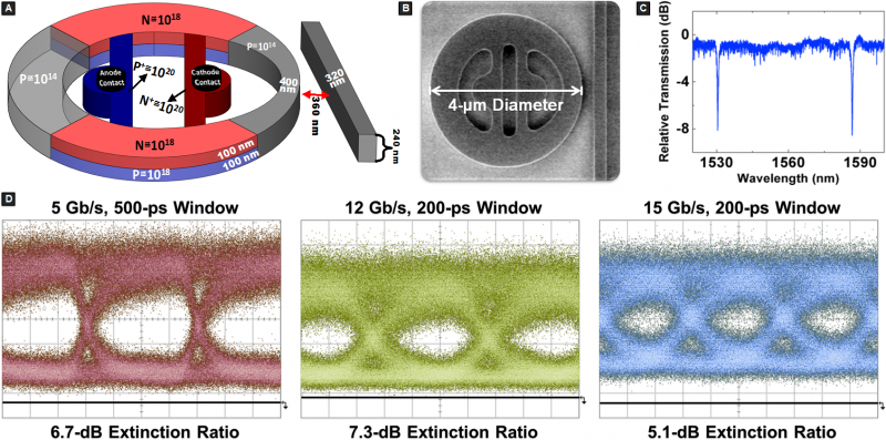
In our work [2] , we demonstrated a new class of modulators, adiabatic resonant microring (ARM) modulators, which enable the integration of vertical p-n junctions and interior contacts while maintaining a high quality factor and compact size, while preserving single radial mode propagation and thereby achieving an uncorrupted FSR. Adiabatic resonant microrings (ARMs) have been shown both numerically [3] and experimentally to enable interior contacts and a compact size while maintaining high quality factors. ARMs operate on the principle of mode-evolution. In the coupling region, the ring waveguide is made narrow to ensure single-mode operation, and the waveguide is then slowly widened to enable contact to the microring where there is no optical field. Here, we demonstrated a vertical p-n junction based on the ARM modulator operating in depletion mode, with data rates up to 12 Gb/s, while occupying less than 12.5 µm2 of chip area and maintaining an uncorrupted 6.9 THz FSR. Figure 1 depicts the device and summarizes the experimental results.

Figure 1: A) 3D diagram of the ARM modulator that we used in these experiments; B) scanning electron micrograph (SEM) of the silicon layer of the ARM modulator; C) measured spectral response showing the uncorrupted FSR (6.9 THz) of the resonator; and D) high-speed output optical eye diagrams for data rates: 5Gb/s (left), 12Gb/s (middle), and 15Gb/s (right).
- M. R. Watts, W. A. Zortman, D. C. Trotter, R. W. Young, and A. L. Lentine, “Vertical junction silicon microdisk modulators and switches,” Opt. Express vol. 19, pp. 21989–22003, 2011. [↩]
- E. Timurdogan, M. Moresco, A. Biberman, J. Sun, W. A. Zortman, D. C. Trotter, and M. R. Watts, “Adiabatic resonant microring (ARM) modulator,” in Proc. Optical Interconnects Conference, TuC6, 2012, pp. 48–49. [↩]
- M. R. Watts, “Adiabatic microring resonators,” Opt. Lett. Vol. 35, pp. 3231–3233, 2010. [↩]