A Monolithic Electronic-photonic Integration Platform in Commercial 45-nm SOI
- Category: Circuits & Systems, Optics & Photonics
- Tags: michael georgas, vladimir stojanovic
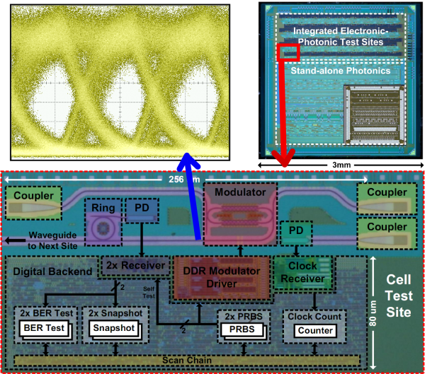
Integrated photonic interconnects present a disruptive alternative to electrical I/O for many VLSI applications, with potential for superior bandwidth density through dense-wavelength-division-multiplexing (DWDM) and energy-efficient operation through both monolithic integration and lower transmission losses. There are two main paths toward an integrated platform. Hybrid designs [1] [2] [3] enable each component to be custom-tailored but penalize energy efficiency due to large parasitic and packaging capacitance. Manufacturing costs can also increase due to requisite process flows and costly 3D integration or microbump packaging. Monolithic integration offers reduced power and cost but has not penetrated deeply scaled technologies due to necessary process customizations. The platform in Figure 1 monolithically integrates all necessary photonic components (vertical grating couplers, ring filters, modulators, and photodiodes) with electronics in a commercial state-of-the-art 45-nm SOI process with no foundry changes. High-speed electrical and optical components are placed with micron-scale proximity on the same die, minimizing interface parasitics without sacrificing performance or commercial scalability. The eye diagram represents the first fully monolithic electro-optic modulation in 45-nm technology, driven by an on-chip double-data-rate modulator driver. The driver is a configurable all-digital push-pull circuit with sub-bit-time pre-emphasis and split supplies. Due to long carrier lifetimes in silicon and relatively long intrinsic region of these particular modulator designs, the rate is limited to 600Mb/s, achievable in both 1280-nm and 1550-nm bands. Further device design and biasing optimization will improve performance into the multi-Gb/s range. Figure 2 shows an 8-ring filter bank with 30-GHz bandwidth wavelength-channels fabricated in order and distributed across a 2.04-THz free spectral range. Integrated sigma-delta heater drivers thermally tune rings to a 250-GHz grid with an efficiency of 2.6mW/nm, compensating for ring-resonance mismatch due to process variation and enabling high bandwidth density through DWDM.
-
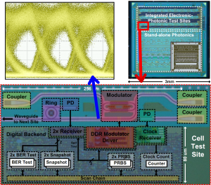
- Figure 1: Platform and link architecture showing photonic components adjacent to CMOS driver and support circuitry. Modulator driver and optical eye diagram at 600 Mb/s and 1550 nm.
-
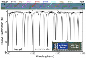
- Figure 2: Through-port transmissivity of a WDM ring filter bank, before (as fabricated) and after being tuned by the on-chip integrated sigma-delta controller for equal channel spacing.

- I. Young, E. Mohammed, J. Liao, A. Kern, S. Palermo, B. Block, M. Reshotko, and P. Chang, “Optical I/O technology for tera-scale computing,” IEEE Int. Solid-State Circuits Conf. Dig., Feb. 2009, pp. 468-469a. [↩]
- A. Rylyakov, C. Schow, B. Lee, W. Green, J. Van Campenhout, Y. Min, F. Doany, S. Assefa, C. Jahnes, J. Kash, and Y. Vlasov, “A 3.9ns 8.9mW 4×4 silicon photonic switch hybrid integrated with CMOS driver,” IEEE Int. Solid-State Circuits Conf. Dig., Feb. 2011, pp. 222-224. [↩]
- F. Liu, D. Patil, J. Lexau, P. Amberg, M. Dayringer, J. Gainsley, H. Moghadam, X. Zheng, J. Cunningham, A. Krishnamoorthy, E. Alon, and R. Ho, “10 Gbps, 530 fJ/b optical transceiver circuits in 40nm CMOS,” IEEE Symp. VLSI Circuits, pp. 290-291, June 2011. [↩]