- Authors: J. Chesin, S. Gradečak
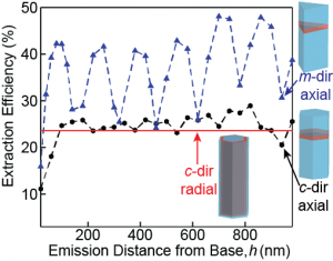
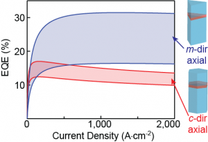
III-nitride nanowire-based light-emitting diodes (LEDs) are promising alternatives to thin-film LEDs for solid-state lighting[]. Facile strain relaxation in nanowires allows epitaxial growth on mismatched substrates, such as silicon[]. We compare the external quantum efficiency of III-nitride LEDs based on axial and radial nanowire heterostructures on silicon substrates, considering many important aspects of the design, including polarization anisotropy common in III-nitrides[] and the effects of orientation with respect to surface recombination and the radiative efficiency of the quantum well. Extraction efficiency was calculated using finite-difference time domain photonic simulations; the internal quantum efficiency (IQE) was estimated based on the relative rates of non-radiative, radiative and Auger recombination. We first note that there are different regimes of wave-guiding, where nanowires can weakly guide a single-mode, strongly confine that mode or guide multiple modes. We focus on single-mode nanowires in which the light is well confined within the nanowire. In such nanowires we find that the placement of the quantum well (QW) where coupling to the fundamental mode is maximized also results in the highest light extraction efficiency. We find that m-directional axial heterostructures have the highest extraction efficiency, due to the strong polarization anisotropy of III-nitrides, which orients emission so as to couple strongly with the fundamental mode (Figure 1). Furthermore, despite higher surface recombination rates, m-directional axial heterostructures display similar or higher IQE than c-directional axial heterostructures due to lower radiative recombination efficiency in polar c-plane QWs caused by the quantum-confined Stark effect. The modeled IQE and the simulated extraction efficiencies are combined to find a range of expected external quantum efficiencies (EQEs), which reveal that m-directional axial heterostructures have EQEs up to three times that of c-directional axial heterostructures at high current densities (Figure 2). This work provides important guidelines for the design of future III-nitride nanowire-based LEDs with high overall efficiencies.
-

-
Figure 1: Simulated extraction efficiency as a function of the QW placement for m-directional and c-directional axial heterostructures, with the solid line indicating the extraction efficiency for a
c-directional radial heterostructure with the QW placed at 0.9 the distance from the center to the surface.
-

-
Figure 2: Estimated EQE ranges for m- and c-directional axial heterostructures obtained by combining IQE modeling (via the A-B-C model) and extraction efficiency simulations from three-dimensional finite-difference time-domain photonic simulations.
- Authors: X. Zhou, M.-Y. Lu (National Chung Cheng University), Y.-J. Lu (National Tsing Hua University), S. Gwo (National Tsing Hua University), S. Gradečak
- Sponsorship: EFRC Center for Excitonics
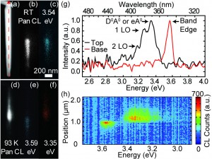
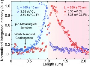
GaN-based nanowires and nanorods are promising materials systems for optoelectronic applications such as high efficiency light emitting diodes[],[] or low lasing threshold lasers[],[]. To improve device design and fabrication based on these nanostructures, nanoscale correlation of heterostructure properties to doping and alloying are essential. We report nanoscale optical investigation of GaN p-n junction nanorods by cathodoluminescence (CL) in scanning transmission electron microscopy (STEM), a non-destructive and facile way to study doping and alloying with high spatial resolution, at both room and cryogenic temperatures. The GaN nanorods were grown by plasma-assisted molecular beam epitaxy (PAMBE) and doped with Si and Mg for respective n- and p-type doping. The position of the Mg acceptor level was identified at 0.24 eV above the valence band by comparing the CL spectra in n- and p-doped GaN in the same nanorod (Figure 1). Intensity profiles of CL emissions characteristic of dopant-related transitions were used to determine precisely the position of the p-n junction. CL quenching inside the nanorod was attributed to structural defects due to nanorod coalescence at the nanowire base and unpassivated surface states in n- and p-doped nanorod portions, respectively. Minority carrier diffusion lengths of 160 nm and 650 nm in Si- and Mg-doped GaN, respectively, were extracted (Figure 2). Temperature-dependent CL study also reveals activation energy of 19 meV for non-radiative recombination in Mg-doped GaN nanorods, which is likely due to surface states. The measured optical emission, dopant level, and estimated carrier diffusion lengths from this study focusing on GaN nanorods are consistent with previous thin film studies. The defect-induced CL quenching highlights the importance of controlling nanorod coalescence during MBE growths and surface passivation for nanostructures to further improve their device performances.
-

-
Figure 1: (a) Dark-field STEM, (b) panchromatic, and (c) 3.54-eV monochromatic CL images of a single GaN p-n junction nanorod taken at RT. (d) Panchromatic, (e) 3.59-eV, and (f) 3.35-eV monochromatic CL images of the same nanorod at 93 K. (d) CL spectra of taken at top and base of the nanorod. (h) CL spectrum map along the length of the nanorod indicated by the dotted line in (a).
-

-
Figure 2: Normalized integrated intensities of the 3.59-eV and 3.35- eV CL luminescence along the length of the nanorod shown in Figure 2(h). The positions of the nanorod coalescence in the n-GaN section and metallurgical junction are indicated. The squares and circles are experimental data and the dashed lines are fits based on an exponential decay model.
- Authors: K. H. Baloch, A. Johnston-Peck, K. Kisslinger, E. Stach, S. Gradečak
- Sponsorship: Department of Energy
Solid state light-emitting diodes (LEDs) containing InxGa1-xN (0 ≤ x ≤ 1)/GaN hetrostructures as active components are of particular importance because of their ability to emit intense light in the entire visible spectrum. However, the cause of their high light-emission efficiency is a matter of debate. Scanning transmission electron microscopy (STEM) and low-loss electron energy loss spectroscopy (EELS) studies conducted at voltages ≥ 200 kV have attributed strong emission to the formation of “large-scale”1-3-nm In-rich clusters[]. However, this finding was questioned in a high resolution transmission electron microscopy (HRTEM) study, which argued that observed spinodal decomposition was caused due to knock-on damage by the 200 kV electron beam[].
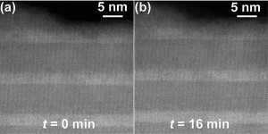
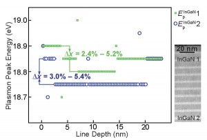
To understand whether or not InGaN alloy in these hetrostructures undergoes spinodal decomposition, we employed atomically resolved aberration (CS)-corrected STEM at 120 kV to demonstrate that this voltage is below the knock-on displacement threshold for InGaN as no discernible electron-beam damage was observed after a continuous exposure for extended periods of time (see Figure 1). To verify whether small contrast variations in the InGaN quantum wells (QWs) seen in Figure 1 correspond to a variation in In composition, ∆x, we employed low-loss EELS at 120 kV. By scanning the electron beam in QWs, identified as InGaN 1 and InGaN 2 in Figure 2, the energy of the plasmon peak (Ep), which is characteristically composition-dependent, is measured with a spatial resolution of 0.3 nm; Ep is plotted in Figure 2. By measuring ∆x, for each of the QWs separately, we determined that the measured changes in plasmon energies correspond to compositional variation of 5.4% or less, which is too small to be attributed to the existence of large-scale In-rich clusters. The next step is to correlate these structural and electronic properties with the optical properties with sub-wavelength resolution by employing a custom cathodoluminescence set-up incorporated in a STEM.
-

-
Figure 1: Time-series of the three InGaN QWs separated by GaN barriers acquired by CS-STEM at 120 kV at (a) t = 0 min and (b) t = 16 min. These images confirm that there is no beam-induced damage at 120 kV.
-

-
Figure 2: Energy of the plasmon peak (Ep) extracted from low-loss EELS data plotted as a function of scan position. The compositional variation corresponding to the observed changes in Ep is < 5.4%, which suggests that there are no large-scale In-rich clusters present.
- Authors: S. Ermez, S. Gradecak
- Sponsorship: NSF
Nanowires combine the intrinsic properties of semiconductors with low dimensionality, which makes them potential building blocks for optoelectronic applications. GaAs nanowires are of particular interest for solar cell applications due to the high absorption coefficient and high electron mobility of GaAs. Common bottom-up nanowire growth methods involve metal seed particles to achieve one-dimensional growth; however, metal seeds can introduce impurities into nanowires that can deteriorate their optoelectronic properties[]. Self-assisted growth mechanism, in which one of elements of nanowire is used as a seed particle, eliminates possible contamination from the seed particles. Self-assisted GaAs nanowires grown via molecular beam epitaxy have been reported in the literature[], but metal-organic chemical vapor deposition (MOCVD) has not been explored so far despite the fact that MOCVD is an industrial-scale technique that can yield high growth rates and high nanowire throughput.
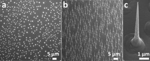
In this study, we have grown GaAs nanowire arrays using in-situ deposited Ga droplets as seed particles. Nanowire growth is realized by a two-step approach in MOCVD: high-temperature in-situ Ga droplet formation followed by low-temperature nanowire growth using Ga droplets as seed particles. The two-step approach has been found crucial; high temperatures are required for efficient Ga precursor decomposition and large surface diffusion length of Ga adatoms, which affect the nanowire density and diameter. On the other hand, lower growth temperatures are necessary to promote one-dimensional growth and to minimize lateral growth on nanowire facets. Nanowire density is around 8×10⁶ nanowires/cm2 as determined from top-view SEM images, such as Figure 1a. Figure 1b shows the nanowire array tilted at 45°, with average nanowire length around 4.6 μm. Nanowires have a tapered geometry due to Ga droplet consumption during growth (Figure 1c). By utilizing in-situ deposited Ga droplets as seed particles, we have achieved contamination-free GaAs nanowire arrays suitable for optoelectronic applications.

Figure 1: (a) Top-view SEM image of GaAs nanowire array showing nanowire density and uniformity. (b) 45° tilted nanowire array reveals average height of nanowires as 4.6 μm. (c) Nanowires have a tapered morphology due to consumption of Ga seed particle.
- Authors: S. Chang, H. Park, J. Jean, J. J. Cheng, P. T. Araujo, M. Wang, M. G. Bawendi, M. S. Dresselhaus, V. Bulović, J. Kong, S. Gradečak
- Sponsorship: Eni S.p.A.
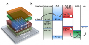
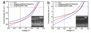
Semiconducting nanowire-based solar cells have gained interest because of their potential to achieve one-dimensional charge transport pathways and large interfacial areas of well-ordered bulk heterojunction geometry[]. Simultaneously, due to the outstanding electrical, mechanical, and optical properties, graphene is being explored as a potential replacement for indium tin oxide (ITO) as a transparent conducting electrode. The growth of semiconducting nanowires on graphene would open up the opportunities to develop flexible solar cell devices, but challenges remain in preserving the structural and electrical properties of graphene during the process. Here, we demonstrate the graphene cathode-based hybrid solar cells composed of ZnO nanowire as an electron transporting layer and two different photoactive materials: conjugated polymers and PbS quantum dots (Figure 1).
The growth of highly uniform, well-aligned ZnO nanowire arrays on graphene is enabled by the interfacial modification with conductive polymer that preserves the structural and electrical properties of grapheme. We developed efficient graphene cathode-based solar cells with the power conversion efficiencies of 4.2% and 0.5% for PbS quantum dot and P3HT polymer structures, respectively, efficiencies that are comparable to the similar ITO-based devices (Figure 2)[],[]. This behavior can be attributed to the interfacial modification of the graphene electrode that facilitates conformal, smooth wetting of the ZnO seed layer and subsequent ordered growth of the ZnO nanowires. The advances demonstrated by this work suggest that graphene can serve as a viable replacement for ITO in various photovoltaic device configurations.
-

-
Figure 1: Hybrid graphene/ZnO nanowire solar cells. (a) Schematic diagram of the graphene cathode hybrid solar cells: graphene deposited on quartz is covered by a polymer (PEDOT:PEG(PC) or RG-1200), followed by the ZnO seed layer and ZnO nanowires. The nanowires are then infiltrated and covered with PbS QDs or P3HT, and finally with MoO3/Au; (b) Flat-band energy level diagram of the solar cells.
-

-
Figure 2: (a) J–V characteristics of the graphene-based PbS QD devices with different polymer interlayers, demonstrating performance comparable to that of an ITO reference cell. (b) J–V characteristics of representative graphene-based P3HT devices with different polymer interlayers, compared with an ITO reference device. Insets in (a) and (b) show SEM cross-section images of the complete devices.
- Authors: E. Jones, D. Cooper, J.-L. Rouviere, A. Béché, M. Azize, T. Palacios, S. Gradečak
- Sponsorship: MIT-MTL GaN Energy Initiative, MISTI France, NSF
Due to its high band gap energy and superb electronic-carrier mobilities, GaN is fast becoming the material of choice for fabricating advanced optical and high-power electronic devices. Nanoribbon-structured high-electron-mobility transistor (HEMT) structures present a novel route towards strain engineering in GaN-based systems, which could lead to enhanced device performance[]. In order to optimize the strain in these devices, however, it is important to quantify the strain in individual nanostructures. This work uses geometric phase analysis (GPA) and nanobeam electron diffraction (NBED) to quantify and map the strain over individual nanoribbon cross-sections, with nanometer resolution providing new insights into device evolution during fabrication inaccessible by other characterization techniques.
Nanoribbon structures were defined between the source and drain of planar HEMT structures using electron-beam lithography and dry-etching techniques. Lattice resolved images of individual ribbons were acquired using high-angular annular dark field (HAADF) and bright field (BF) scanning TEM (STEM) for GPA while line scans of NBED patterns were obtained from three different structures. Strain profiles were also simulated using a previously developed finite element analysis (FEA) model[] for comparison to the experimental profiles.
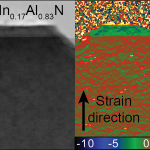
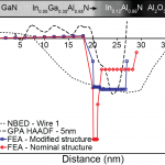
Figure 1 shows a BF STEM image of a typical ribbon structure studied in this work with corresponding growth direction strain map. From this map a growth direction strain of -2.7% ± 0.5% with respect to the GaN substrate is measured in the HEMT layers. These measurements are confirmed by the NBED strain profiles, which also measure a strain of -2.7% ± 0.1% but with a precision five times greater than GPA. The experimental results suggest that the nominal compositions of the HEMT layers (see Figure 1) are not accurate. Use of linear elastic theory and energy dispersive X-ray spectroscopy enables calculation of the actual composition of each HEMT layer, which significantly improves strain profiles predicted by FEA as seen in Figure 2.
-

-
igure 1: BF STEM image of a typical nanoribbon-structured HEMT studied in this work with layers labeled with nominal compositions. GPA is used to generate a map of the strain over the whole structure, clearly showing the strained HEMT layer.
-

-
Figure 2: Comparison of experimental and simulated strain profiles obtained from GPA, NBED, and FEA. The two simulated strain profiles demonstrate how the revised chemistries seen in the inset improved the FEA model.
