Jesús A. del Alamo
Collaborators
- J. Jimenez, Triquint Semicon
- D.H. Kim, Teledyne
- Y. Knafo, Gal El
- A. Valdes, IBM
Postdoctoral Fellow
- J. Joh
- T. W. Kim
Graduate Students
- U. Gogineni, Res. Asst., EECS
- D.H. Jin, Res. Asst., EECS
- L. Xia, Res. Asst., EECS
- S. Demirtas, Res. Asst., EECS
- X. Zhao, Res. Asst., DMSE
- A. Guo, Res. Asst. EECS
- J. Lin, Res. Asst. EECS
Support Staff
E. Kubicki, Admin. Asst. II
Publications
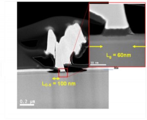
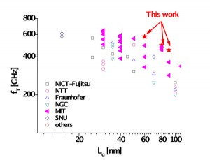
Kim, T.-W., D.-H. Kim, and J. A. del Alamo, “60 nm Self-Aligned-Gate InGaAs HEMTs with Record High-Frequency Characteristics,” IEEE International Electron Devices Meeting, San Francisco, CA, December 6-8, 2010, pp. 696-699.
Kim, D.-H., J. A. del Alamo, P. Chen, W. Ha, M. Urteaga and B. Brar, “50 nm E-Mode In0.7Ga0.3As PHEMTs on 100 mm InP Substrate with fmax>1 THz,” IEEE International Electron Devices Meeting, San Francisco, CA, December 6-8, 2010, pp. 692-695.
Joh, J. and J. A. del Alamo, “RF Power Degradation of GaN High Electron Mobility Transistors,” IEEE International Electron Devices Meeting, San Francisco, CA, December 6-8, 2010, pp. 468-471.
Joh, J., P. Makaram, C. V. Thompson, and J. A. del Alamo, “Planar View of Structural Degradation in GaN High Electron Mobility Transistors: Time and Temperature Dependence,” Invited talk at International Workshop on Nitride Semiconductors (IWN 2010), Tampa, FL, 2010.
Kim, D.-H. and J. A. del Alamo, ”30 nm InAs PHEMTs with fT=644 GHz and fmax=681 GHz,” IEEE Electron Device Letters, vol. 31, no. 8, pp. 806-808, August 2010.
Kim, D.-H. and J. A. del Alamo, ”Scalability of sub-100 nm InAs HEMTs on InP Substrate for Future Logic Applications,” IEEE Transactions on Electron Devices, vol. 57, no. 7, pp. 1504-1511, July 2010.
Makaram, P., J. Joh, J. A. del Alamo, T. Palacios, C. V. Thompson, ”Evolution of Structural Defects Associated with Electrical Degradation in AlGaN/GaN HEMTs,” Applied Physics Letters, vol. 96, p. 233509, 2010.
Wu, J. H., and J. A. del Alamo, ”Fabrication and Characterization of through-Substrate Interconnects,” IEEE Transactions on Electron Devices, vol. 57, no. 6, pp. 1261-1268, June 2010.
Kim, T.-W., D.-H. Kim and J. A. del Alamo, “Logic Characteristics of 40 nm thin-channel InAs HEMTs,” 22nd International Conference on Indium Phosphide and Related Materials, Kagawa, Japan, May 31-June 4, 2010, pp. 496-499.
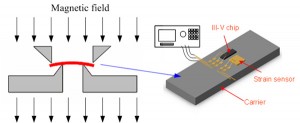
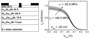
Xia, L. and J. A. del Alamo, “Mobility enhancement in Indium-rich N-channel InxGa1-xAs HEMT by Application of <110> Uniaxial Strain,” 22nd International Conference on Indium Phosphide and Related Materials, Kagawa, Japan, May 31-June 4, 2010, pp. 504-507.
Joh, J. and J. A. del Alamo, “Reliability and Failure Mechanisms of GaN-based HEMTs,” Invited talk at 10th Expert Evaluation and Control of Compound Semiconductor Materials and Technologies (EXMATEC 2010), Darmstadt/Seeheim, Germany, May 19-21, 2010, pp. 57-58.
Joh, J., J. A. del Alamo, K. Langworthy, S. Xie, and T. Zheleva, “Correlation between electrical and material degradation in GaN HEMTs stressed beyond the critical voltage,” Microelectronics Reliability, vol. 51, pp. 201-206 (2011).
Demirtas, S. and J. A. del Alamo, “Effect of Trapping on the Critical Voltage for Degradation in GaN High Electron Mobility Transistors,” 2010 International Reliability Physics Symposium, Anaheim, CA, May 2-6, 2010, pp. 134-138.
Gogineni, U., H. Li, J. A. del Alamo, S. Sweeney, J. Wang, and B. Jagannathan, ”Effect of Substrate Contact Shape and Placement on RF Characteristics of 45 nm Low Power CMOS Devices,” IEEE Journal of Solid State Circuits, vol. 45, no. 5, pp. 998-1006, May 2010.
del Alamo, J. A. and D.-H. Kim, “The prospects for 10 nm III-V CMOS,” Invited talk at 2010 International Symposium on VLSI Technology, Systems and Applications (VLSI-TSA), Hsinchu, Taiwan, April 26-28, 2010, pp. 166-167.
Gogineni, U., J. A. del Alamo, and C. Putnam, “RF Power Potential of 45 nm CMOS Technology,” 10th Topical Meeting on Silicon Monolithic Integrated Circuits in RF Systems (SiRF 2010), New Orleans, LA, January 11-13, 2010, pp. 204-207.
Waldron, N., D.-H. Kim and J. A. del Alamo, ”A Self-Aligned InGaAs HEMT Architecture for Logic Applications,” IEEE Transactions on Electron Devices, vol. 56, no. 1, pp. 297-304, January 2010.
