- Authors: Y.-H. Chen, C. Sun, B. R. Moss, M. Georgas, J. Leu, J. Orcutt, Y. Lee, M. Planas, J. Shainline, K. Mehta, J. Sun, H. Li, E. Timurdogan, S. Urosevic, J. Wang, M. Weaver, K. Asanović, M. Watts, M. Popović, R. Ram, V. Stojanović
- Sponsorship: CICS, DARPA, NSF, SRC/FCRP IFC, Trusted Foundry, Natural Sciences and Engineering Research Council of Canada
Integrated photonic interconnects enable new possibilities for bandwidth and energy-efficiency driven VLSI applications, such as many-core processor systems, by removing the perennial memory bandwidth bottleneck[]. Though both heterogeneous[][][] and monolithic[] electronic-photonic platforms have been proposed, monolithic integration remains the preferred choice due to lower interface parasitics and manufacturing costs.
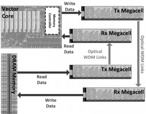
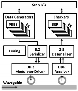
This work will demonstrate an optical processor-memory platform, as shown in the block diagram of Figure 1, which consists of two chips fabricated in two different processes. The DRAM memory chip, implemented in a quarter-micron-equivalent CMOS bulk process, contains both single-wavelength link and wavelength-division multiplexing (WDM) link test sites, called a Megacell. The processor chip, manufactured on a commercial 45-nm SOI process, features a custom vector processor that can use the on-chip WDM link Megacell structure to optically communicate to an emulated DRAM structure. Both chips monolithically integrate photonic link components (vertical grating couplers, ring filters, modulators, and photodiodes) with drivers and synthesized backend circuitry. For link characterization, each Megacell, as shown in Figure 2, contains on-chip pseudorandom binary sequence (PRBS) data generators to feed modulators as well as a bit-error-rate (BER) check receiver backend. Programmable thermal tuning controllers were also added to compensate for process and thermal-induced mismatches in ring resonant devices.
-

-
Figure 1: The processor-DRAM interface platform, which consists of a DRAM memory chip and a processor chip with an on-chip Megacell structure and off-chip optical links.
-

-
Figure 2: A single transceiver site of the Megacell structure in the DRAM memory chip. The generated PRBS data is modulated through the link and then BER-checked at the receiver side.
- Authors: H. Fariborzi, F. Chen, R. Nathanael, J. Jeon, L. Hutin, T. K. Liu, V. Stojanović
- Sponsorship: DARPA, CICS, SRC/FCRP C2S2, SRC/FCRP MSD
Silicon CMOS circuits have a well-defined lower limit on their achievable energy efficiency due to sub-threshold leakage. Once this limit is reached, power constrained applications will face a cap on their maximum throughput independent of their level of parallelism. Avoiding this roadblock requires an alternative device with a steeper sub-threshold slope, i.e., lower VDD/Ion for the same Ion/Ioff. One promising class of such devices is electrostatically actuated nano-electro-mechanical (NEM) switches with nearly ideal Ion/Ioff characteristics. Although mechanical movement makes NEM switches significantly slower than CMOS, they can be useful for a wide range of VLSI applications if we reexamine traditional system- and circuit-level design techniques to take advantage of the electrical properties of the device.
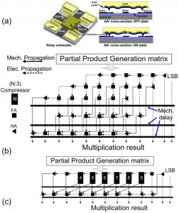
Basic circuit design techniques and functionality of some main building blocks of VLSI systems, such as logic, memory, and clocking structures, have been demonstrated in our previous works[][][]. Recently, by employing pass-transistor logic design, we have designed and demonstrated complex relay-based arithmetic units such as multipliers (Figure 1b-c)[]. Simulation results of an optimized 16-bit relay multiplier built in a 90-nm equivalent relay process model predict ~10x improvement in energy-efficiency over optimized CMOS designs in the 10-100 MOPS performance range. The relative performance of the multiplier enhancements are in line with what was previously predicted by a NEM relay 32-bit adder[], suggesting that complete VLSI systems, such as a microprocessor, would expect to see similar energy/performance improvements from adopting NEM relay technology[],[].
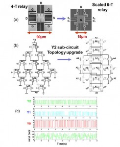
Since scaling is crucial for performance, energy, and total area improvement, we have developed a scaled version of the original relay, a 6-terminal relay, which is 25x smaller and offers enhanced functionality. The operation of the main building block of the NEM-relay based multiplier, the (7:3) compressor, built with these scaled devices is experimentally demonstrated. This circuit, consisting of 46 scaled relays, is the largest scaled relay circuit successfully tested to date (Figure 2).
-

-
Figure 1: (a) The 4T NEM relay and its operating states, (b) a 6-bit relay multiplier built with full and half adders, and (c) an alternative design built with (7:3) and smaller compressors.
-

-
Figure 2: (a) The original 4T and the scaled 6T devices and their symbols, (b) the MSB sub-circuit of the (7:3) compressor and the updated topology for the 6T relay, and (c) experimental results of the full 6T compressor.
- Authors: J. Leu, B. Moss, C. Sun, M. Georges, Y. Chen, D. Yost, M. Watts, V. Stojanovic
- Sponsorship: DARPA
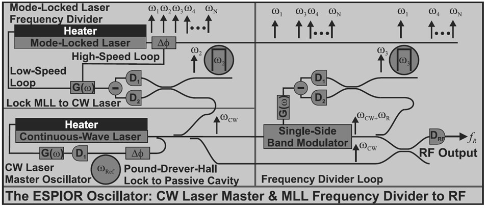
A novel device, erbium silicon photonic integrated oscillators and radar (ESPIOR), is composed of state-of-the-art silicon photonics and erbium-ytterbium based laser oscillators, integrated onto a CMOS wafer with 1fF capacitance 3D vias[], in conjunction with hybrid attached optical components including a pump laser, an optical isolator, and a saturable absorber. ESPIOR uses a unique combination of a low phase noise continuous-wave (CW) distributed feedback (DFB) laser master oscillator, and a mode-locked laser (MLL) frequency divider to achieve a low phase noise 20-GHz microwave carrier. A schematic of the complete system is shown in figure 1.
To implement the design across the photonic wafer and CMOS wafer, a merged design environment was created. Photonic devices were drawn as parameterized cells and then treated as macro blocks that could be placed throughout the chip using scripts. For verification, design rules were added to ensure the manufacturing yield of the 3D vias that connect the circuits with the photonic devices. Layout-vs-schematic (LVS) rules were used to compare the netlist including photonic components to the integrated layout, where each contact of the photonic devices was labeled.
To test the individual photonic/electric building blocks of the ESPIOR, we have test sites for photodiodes connected with transimpedance amplifiers, linear modulators and phase shifters connected to driver circuits, switches, lasers, etc. Many combinations of design types were implemented, enabling us to test the performance tradeoffs in various designs. For instance, the driver circuit for the linear modulator was designed at different bandwidth specifications. Also, the modulator itself has travelling wave vs. lumped capacitance variants. As a demonstration of the integrated platform separate from the ESPIOR, a digital CMOS section was implemented; in it, many modulators, switches and photodiodes are connected in various link configurations. The analog CMOS transmitter and receiver frontends are highly configurable and can perform on-chip bit-error-rate testing.

Figure 1: A diagram of the ESPIOR oscillator, which utilizes the low phase noise properties of a continuous-wave laser as a master oscillator and a mode-locked laser as a frequency divider.
- Authors: O. Abari, F. Chen, F. Lim, A. Chandrakasan, V. Stojanović
- Sponsorship: NSF, Natural Sciences and Engineering Research Council of Canada
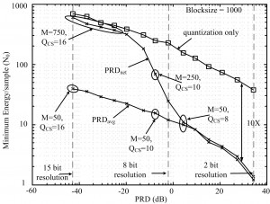
Compressed sensing (CS) is a sub-Nyquist sampling technique[] with under-explored implementation potential. In this multi-disciplinary project, we analyze CS circuit architectures from a hardware implementation perspective[],[], develop and apply end-to-end evaluation methodologies from a system perspective[],[], and support experiments by analyses from a theoretical perspective[]. We have considered the practical aspects of CS applied to both wireless sensors and Analog Information Converters (AICs). For the former, we showed that a digital CS-based sensor system is efficient and robust. By data compression alone, CS enables over 10X energy reduction in transmission energy; see Figure 1. CS is robust to channel errors, and amenable to simple schemes to enable 4X energy reduction[]. For the latter (AICs), we evaluated the ability of CS to overcome resolution/performance limitations of Nyquist-rate high-speed sampling (limited by jitter, aperture and other circuit impairments). We find AICs have no performance advantage over high-speed ADCs. In standard architectures, signal encoding is realized with a mixer-like circuit, which still operates at Nyquist frequency to avoid input aliasing. Our evaluation shows that AICs are resolution limited, though they may enable a 2x energy reduction for low amplifier gains and very sparse signals[].
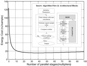
There is little literature on CS recovery hardware. As an initial step, we explored the implementation design space for a matching pursuit (MP) algorithm; see Figure 2 (insert)[]. We chose MP as it is the simplest possible recovery algorithm, so that we may gain critical first insights. MP is a greedy (iterative) algorithm that estimates a sparse sample in each iteration and produces the full estimate once it halts. The figure also shows the basic implementation blocks where we found that the max-correlation unit, which consists of multipliers, dominates the energy expenditure. The energy-cost evaluation in Figure 2 shows diminishing returns around 20 multipliers, at 1 V supply, in 45-nm CMOS technology. Overall, at 8 bits resolution and 10 fixed iterations, the energy cost of recovery is 2.8 nJ/sample, with an area of 0.4 mm2 at a minimum-energy throughput of 2.5 mega-samples/s at 0.4 V supply. Since the algorithm is block-parallel, a further throughput increase comes with a linear increase in area.
-

-
Figure 1: Minimum energy versus percent RMS difference (PRD). Compared average (PRDavg) and worst (PRDnet) distortions,
optimized over compression rate (M) and quantization (QCS).
-

-
igure 2: Matching pursuit. Energy-cost evaluation finds flattening of minimum energy curve, dominated by multipliers in the correlation block. Nominal 1 V supply, 45-nm process.
- Authors: A. Suleiman, R. Sredojević, V. Stojanović
- Sponsorship: Intel
As CMOS technology scales down and the need for higher data rates increases, non-ideal channel characteristics play a critical role in limiting the speed. Equalization is a well-known method to overcome band-limited channels and reflections[]. Most high-speed links apply transmitter equalization using a finite impulse response feed forward equalizer (FFE), with an optional decision feedback equalizer (DFE) at the receiver[],[].
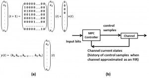
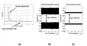
This work proposes a new nonlinear equalization method using a model predictive control (MPC) algorithm. MPC is a class of control algorithms in which the current control action is obtained by solving online, perhaps approximately, an open-loop optimal control problem. One important advantage of MPC in peak-power constrained link environment is its ability to cope with hard constraints on controls and states[]. Figure 1 shows how this algorithm is used; the channel is modeled as an FIR (Figure 1a) filter, which enables feeding back channel states to the MPC controller to solve the optimization problem (Figure 1b). Knowing the state of the channel enables a very fine nonlinear equalization.
MPC equalization significantly outperforms traditional FIR-based equalizers by more than 63% increase in eye opening height as shown in figure 2. Interestingly, the more the channel is dispersed in time and suffers from reflections, the more improvement MPC can achieve. The complexity of this algorithm is the main challenge in implementations; however, techniques can be applied to design hardware MPC equalizers with reasonable area and power budgets, by sacrificing some performance gains. The main candidate is a RAM-DAC implementation[], which can achieve equalization and compensate for any timing mismatches or DAC non-linearity.
-

-
Figure 1: Modeling the equalization problem: (a) channel state-space representation, (b) block diagram for MPC algorithm. Note that the MPC controller is a function of input bits (horizon) and channel current state.
-

-
Figure 2: (a) Pulse response of 3 inches backplane channel @ 8 Gbps[] . (b) Channel output with 20-tap FIR equalizer. (c) Channel output with MPC equalizer.
- Authors: C. Sun, E. Timurdogan, M. R. Watts, V. Stojanović
- Sponsorship: DARPA, NSF
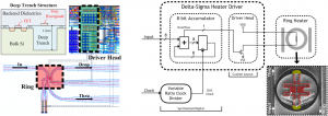
Wavelength-division multiplexed (WDM) silicon-photonic links form a promising alternative to traditional electrical interconnects. However, the essential component of these WDM networks, the microring resonator, suffers from resonance drifts due to either static process variations or dynamic temperature fluctuations, necessitating methods for active resonance tuning[],[]. In this work, we demonstrate a heater driver system for microring resonators consisting of a fully-digital Δ∑-based heater driver circuit and an ARM filter (Figure 1, left), both monolithically integrated in a commercial 0.25-µm-equivalent bulk CMOS process with deep-trench isolation capability. Integration of the heater driver alongside the integrated heater minimizes the parasitic resistance from the driver to the heater, provides a digital heater control interface through which multiple rings can be controlled on-chip, and eliminates the dedicated pads for external heater control used in the majority of previous work.
The driver circuit consists of a synthesized pipelined accumulator and a custom one-transistor driver head (Figure 1, right). The circuit utilizes pulse density modulation (PDM) to output a heater drive waveform consisting of a digital pulse train, with a duty-cycle corresponding to an 8-bit digital input setting. The clock frequency of the driver can be used to trade-off the backend power overhead with the size of the digital ripples. The 6-μm diameter ARM filter[] is made using Poly-Si waveguides above deep oxide trenches (Figure 1, left) and achieves an uncorrupted free spectral range (FSR) of 3.7THz (Figure 2, left). Using a process-compatible supply voltage of 2.5V, the system is able to tune the resonance by 350GHz, with an efficiency of 10-15µW/GHz (Figure 2, right).
-

-
Figure 1: Layout of the integrated heater driver connected to the ARM filter, both integrated in a deep trench CMOS process (left). Block diagram of the Δ∑-based heater driver with SEM of the connected ARM filter (right).
-

-
Figure 2: Optical response of the ring filter at minimum and maximum heater power settings (left) and tuning cost per gigahertz, with driver cost included, to reach a specific tuning offset (right).
- Authors: B. R. Moss, C. Sun, M. Georgas, J. Shainline, J. S. Orcutt, J. C. Leu, M. Wade, H. Li, R. Ram, M. A. Popović, V. Stojanović
- Sponsorship: DARPA, NSF, SRC/FCRP IFC, Trusted Foundry, CICS, Natural Sciences and Engineering Research Council of Canada
A monolithically integrated photonic modulator and driver circuit is a key building block toward realizing a dense and energy-efficient communication fabric that can satisfy future bandwidth density demands in VLSI systems.
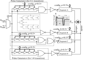
The optical modulator device is a resonant ring with rib waveguide carrier-injection phase shifters, identical to the one in[]. The DDR driver in Figure 1 is designed as an all-digital push-pull circuit with configurable drive strengths, sub-bit-time pre-emphasis[] and split supplies, operating over a range of drive current profiles required for a wide variety of optical devices. The split power supply and level-shift drivers allow exploration of the tradeoffs between energy-cost and extinction ratio. The highly configurable driver back-end controls four independent drive heads, each providing a configurable drive strength and specialized biasing regime. As illustrated in the Figure 1 inset, a combination of drive segments A and B provides the strongest drive generating the sub-bit current pre-emphasis needed for fast injection of carriers into the modulator on a “0” to “1” transition. Reduced strength segment B maintains the lower current levels necessary for keeping the carriers inside the modulator during a logic “1,” replacing carriers lost in recombination. On a “1” to “0” transition, segment D provides a fast reverse-bias period, enabling carrier discharge from the modulator. After the brief discharge period, the modulator is weakly forward-biased into the subthreshold through segment C, lowering the on-resistance of the modulator intrinsic region and allowing faster turn-on “0” to “1.” The final drive heads and optical eye diagram are shown in Figure 2. In combination with the forward and reverse-bias sub-bit pre-emphasis, the weak subthreshold forward biasing speeds up the device an order of magnitude above its inherent bandwidth.
The modulator and its driver, operating at 2.5 Gb/s and 1.23 pJ/b with an extinction ratio of 3dB, demonstrate the fastest, most energy-efficient monolithically integrated driver/modulator in sub-100-nm CMOS technology to date.
-

-
Figure 1: Modulator and driver circuit fed by an on-chip 32-bit pseudo-random bit sequence generator.
-

-
Figure 2: Final driver segments and 2.5 Gb/s eye diagram at 1.23 pJ/b and extinction ratio of 3 dB. An off-chip tunable laser provides the incoming 1550-nm-band light.
- Authors: R. Sredojevic, A. C. Wright, V. Stojanovic
- Sponsorship: SRC/FCRP C2S2, CICS
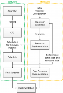
Significant effort is spent researching hardware and software acceleration of basic building blocks for numerical computation[][][]; however, the majority of the previous work focuses on either hardware or software independently. In this work we develop hardware and software together, as shown in Figure 1, providing tight design-time coupling between them, with the ultimate goal of exploring numerical hardware platform tradeoffs at both limits of performance: high speed and low power.
For tight coupling of the algorithm and processor physical layer constraints, our project is centered on the link between these layers: an optimizing compiler. Algorithm optimization begins with synthesizing the computation graph from the written algorithm. Next the graph is optimized through constant folding, dead-code elimination and similar compiler techniques. Additionally tree-rebalancing optimizations are performed to allow for serial associative operations to occur in parallel. Extensive scheduling sweeps are then performed for various processor microarchitectures to find the optimal software/hardware pair. The specifications are fed to an abstract processor template to generate a custom processor similar to the one shown in Figure 2 to run the optimal software. This processor template is written in Bluespec to allow us to postpone decisions on a number of details such as the number and types of processing units, the number and size of memories, the pipeline depths of the floating-point units, and the interconnect structure.
The generated processors are currently synthesized onto a prototyping FPGA platform to confirm our compiler predictions. We see a strong run-time dependence on processor microarchitecture for a given algorithm. Reductions up to 4x in overall latency can be obtained by proper processor configuration, validating a meta-programming approach to processor logic-level design. Furthermore, we show that the optimal latency point is neither at the minimum cycle count nor at the highest clock frequency, but somewhere in between that depends on the topology of the computational flow graph.
-

-
Figure 1: The design process for optimized hardware and software for computation applications.
-

-
Figure 2: Architecture of a custom numerical computation processor generated by the processor template.
