Photonic Processor-DRAM Interface
- Category: Circuits & Systems, Optics & Photonics
- Tags: vladimir stojanovic, yu-hsin chen
Integrated photonic interconnects enable new possibilities for bandwidth and energy-efficiency driven VLSI applications, such as many-core processor systems, by removing the perennial memory bandwidth bottleneck[1]. Though both heterogeneous[2][3][4] and monolithic[5] electronic-photonic platforms have been proposed, monolithic integration remains the preferred choice due to lower interface parasitics and manufacturing costs.
This work will demonstrate an optical processor-memory platform, as shown in the block diagram of Figure 1, which consists of two chips fabricated in two different processes. The DRAM memory chip, implemented in a quarter-micron-equivalent CMOS bulk process, contains both single-wavelength link and wavelength-division multiplexing (WDM) link test sites, called a Megacell. The processor chip, manufactured on a commercial 45-nm SOI process, features a custom vector processor that can use the on-chip WDM link Megacell structure to optically communicate to an emulated DRAM structure. Both chips monolithically integrate photonic link components (vertical grating couplers, ring filters, modulators, and photodiodes) with drivers and synthesized backend circuitry. For link characterization, each Megacell, as shown in Figure 2, contains on-chip pseudorandom binary sequence (PRBS) data generators to feed modulators as well as a bit-error-rate (BER) check receiver backend. Programmable thermal tuning controllers were also added to compensate for process and thermal-induced mismatches in ring resonant devices.
-
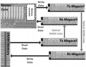
- Figure 1: The processor-DRAM interface platform, which consists of a DRAM memory chip and a processor chip with an on-chip Megacell structure and off-chip optical links.
-
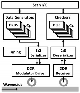
- Figure 2: A single transceiver site of the Megacell structure in the DRAM memory chip. The generated PRBS data is modulated through the link and then BER-checked at the receiver side.
- S. Beamer, C. Sun, Y-J. Kwon, A. Joshi, C. Batten, V. Stojanović, and K. Asanović, ”Re-architecting DRAM with Monolithically Integrated Silicon Photonics,” Int’l Symposium on Computer Architecture (ISCA-37), pp. 129-140, June 2010. [↩]
- I. Young, E. Mohammed, J. Liao, A. Kern, S. Palermo, B. Block, M. Reshotko, and P. Chang, “Optical I/O technology for tera-scale computing,” IEEE International Solid-State Circuits Conference – Digest of Technical Papers, pp.468-469,469a, Feb. 2009. [↩]
- A. Rylyakov, C. Schow, B. Lee, W. Green, J. Van Campenhout, Y. Min, F. Doany, S. Assefa, C. Jahnes, J. Kash, and Y. Vlasov,” A 3.9ns 8.9mW 4×4 silicon photonic switch hybrid integrated with CMOS driver,” IEEE International Solid-State Circuits Conference – Digest of Technical Papers, pp. 222-224, Feb. 2011. [↩]
- F. Liu, D. Patil, J. Lexau, P. Amberg, M. Dayringer, J. Gainsley, H. Moghadam, X. Zheng, J. Cunningham, A. Krishnamoorthy, E. Alon, and R. Ho, “10 Gbps, 530 fJ/b optical transceiver circuits in 40 nm CMOS,” IEEE Symposium on VLSI Circuits, pp. 290-291, June 2011. [↩]
- J. Orcutt, B. Moss, C. Sun, J. Leu, M. Georgas, J. Shainline, E. Zgraggen, H. Li, J. Sun, M. Weaver, S. Urošević, M. Popović, R. J. Ram, and V. Stojanović, “Open foundry platform for high-performance electronic-photonic integration,” Optics Express, vol. 20, no. 11, pp. 12222-12232, May 2012. [↩]