- Authors: A. Guo, J. A. del Alamo
- Sponsorship: SRC/FCRP MSD
Deeply scaled III-V MOSFETs have demonstrated logic performance at 0.5 V, exceeding that of Si [] . The gate length of modern III-V MOSFETs has been recently reduced to sub-100-nm dimensions. However, the actual contacts in current research devices still are many times larger than this. Going forward, a key element for a high-performance, small-footprint III-V CMOS technology is the achievement of nanometer-scale source and drain contacts with low contact resistance. This goal is challenging because as the contact length decreases to the nanometer regime, the contact resistance is expected to increase dramatically. This study focuses on characterizing nanometer-scale metal contacts to III-V heterostructures.
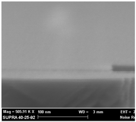
We have first developed a fabrication process to build nano-TLM structures with different contact length (Lc) and spacing (d). We have used Mo contacts to an InGaAs-based heterostructure. Mo definition was achieved by electron-beam lithography followed by dry etching. The mesa and contact pads were formed using photo lithography and a series of dry etching and lift off processes. Figure 1 shows a fabricated nano-TLM structure with ~160-nm contact length and a spacing of ~440 nm. The devices are being characterized using Kelvin (4-terminal) measurements. The sheet resistance of Mo film needs to be considered because the film thickness is decreased to ~50 nm. The contact resistance (Rc) and metal sheet resistance (Rshm) can be extracted using an equivalent circuit model developed for this specific nano-TLM structure. In the future we will expect to integrate nano-scale ohmic contact into a III-V CMOS process, with the goal of reducing transistor footprint and provide insight into the limitations that nano-scale contacts impose on transistor characteristics.

Figure 1: Plan view image of a nano-TLM structure with ~160-nm contact length Mo contacts about ~440 nm apart.
- Authors: L. W. Guo, J. A. del Alamo
As CMOS technology continues to scale to the nanometer regime, there has been a strong demand for alternative materials to replace silicon. III-V materials, in particular, have shown great promise in extending the road map for high-performance CMOS technology because of their superior electron transport properties [] . However, many III-V FETs are still fabricated using wet etchants that are difficult to control and give large undercuts, decreasing their feasibility for use in commercial logic applications that require very tight footprints. In addition, oversized gate-source and gate-drain separations result in parasitic series resistances that play a large role in degrading device characteristics. A great need exists for a low-damage and highly anisotropic dry-etch process for scaled logic III-V FETs.
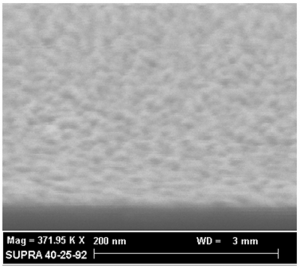
This study explored a dry-etching technique for InGaAs caps using CH4-based chemistry with the addition of SF6. While a CH4/H2 dry etch chemistry gave relatively anisotropic sidewalls with minimal undercut, it was found that this chemistry alone gave rough surfaces, shown in Figure 1. With the addition of SF6 to the discharge, the surface roughness of etched InGaAs was reduced significantly without affecting anisotropy, shown in Figure 2. Furthermore, when the same CH4/H2 dry etch without SF6 was performed on a GaAs surface, it was found to give smooth surfaces, suggesting that the rough surface could be attributed to the formation of indium-based residue
Besides improving the surface roughness of InGaAs dry etching, the addition of SF6 to the CH4/H2 plasma can also promote the use of InAlAs as an etch stop through the formation of AlF3 compounds upon reaching the InAlAs surface [] . However, a drawback to the use of SF6, and many fluorine-containing compounds, is that it attacks silicon oxide and silicon nitride, reducing the effectiveness of these materials as dry-etching masks.
Our research will continue to explore selective dry etching chemistries for III-V heterostructures that provide smooth, highly anisotropic sidewalls with low damage.
-
-
Figure 1: Surface of an InGaAs sample after a 20-min dry etch using CH4/H2 chemistry with an ECR power of 200W.
-

-
Figure 2: The addition of SF6 to the CH4/H2 chemistry appreciably improves the smoothness of etched InGaAs surfaces.
- Authors: S. Warnock, J. A. del Alamo
- Sponsorship: SRC/FCRP MSD
As silicon MOSFETs approach the limits of their capabilities, III-V field-effect transistors show promise to replace them. The low-effective mass of various III-V materials such as InGaAs and InAs gives rise to extraordinarily high electron velocities [] . III-V based High-Electron Mobility Transistors (HEMTs) represent a great model system to understand physics of relevance to future III-V MOSFETs. In HEMTs it is known that as the gate length is reduced to the sub-100-nm regime, the device enters the ballistic regime [] . In this project, a comprehensive ballistic transport model is being developed to enable the analysis of nanometer-scale III-V HEMTs and MOSFETs and predict the performance of scaled transistors.
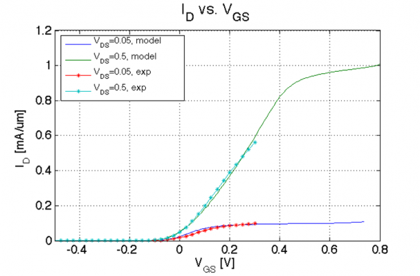
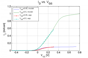
The model uses, at its core, a one-dimensional, self-consistent Poisson-Schrödinger simulation of the heterostructure of the transistor. We then add extrinsic device parameters such as source and drain parasitic resistances (RS and RD), as well as appropriate values for the drain-induced barrier lowering (DIBL) and a distribution of interface trap states across the bandgap at the semiconductor surface (Dit). The model uses ballistic transport theory to calculate the current-voltage characteristics of the device. Next, we can display the corresponding transconductance, transfer characteristics, output characteristics, or C-V characteristics. Using an option to graph experimental data on top of simulated data, we can adjust the extrinsic device parameters to fit the simulations to the experiments or to identify discrepancies between the two that indicate where more refined models are needed. In this development phase of the model, we are using HEMTs to calibrate the model’s validity in the various regimes of operation, after which physics of relevance to III-V MOSFETs, such as the effect of Dit and imperfect ballisticity, will be added. Ultimately, our modeling approach will allow us to easily characterize current and future MOSFETs.
-
-
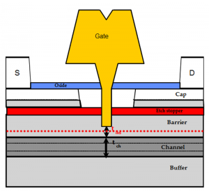
Figure 1: Schematic of a HEMT structure modeled in this work [] . The red dotted line in the schematic indicates the location of the δ doping layer, and the channel consists of a composite of InGaAs and InAs. In the simulations shown in Figure 2, a channel of 5-nm InAs was used.
-
-
Figure 2. Experimental versus theoretical transfer characteristics of the HEMT device in Figure 1. Experimental Lg = 30 nm, RS, RD = 240 Ω·μm, DIBL = 80 mV/V, SS = 80 mV/dec. Model RS = 140 Ω·μm, RD = 270 Ω·μm, DIBL = 50 mV/V.
- Authors: P. Sharma, M. T. Bulsara, E. A. Fitzgerald
- Sponsorship: ARO
Photovoltaics and sustainability have received much attention lately. We seek a tandem photovoltaic device using silicon as both the substrate and lower cell and GaAsP as the upper cell. The ideal band gaps for this two-cell tandem structure with silicon at 1.1eV and GaAsP at 1.75 eV allow access to the highest efficiency possible for a two-cell tandem, 36.5%. The lattice mismatch between GaP and Si is 0.37%; therefore, these two materials constitute a nearly ideal combination for the integration of Si and III–V semiconductor-based technologies. Nevertheless, defect-free heteroepitaxy of GaP on Si has been a major challenge.
One can envision a process in which a Si1-xGex graded buffer is grown on a Si wafer to extend the lattice parameter part of the way to GaAs, at which point a lattice-matched GaAsyP1-y is grown on the Si1-xGex surface, followed by tensile grading of the GaAsyP1-y until GaP is reached. Identifying the composition where the transition can be made from Si1-xGex to GaAsyP1-y depending on the application is an integral objective of this study. This identification will provide the flexibility to engineer the lattice constants from Si to Ge and GaP to GaAs while maintaining low threading dislocation density (TDD) and surface morphology suitable for device processing. This study has achieved the successful growth of high-quality lattice-matched GaAsyP1-y on Si0.5Ge0.5, Si0.4Ge0.6, and Si0.3Ge0.7 virtual substrates. Various characterization techniques clearly reveal a high-quality crystalline interface (Figure 1) between Si1-xGex and GaAsyP1-y with low TDD suitable for device processing, no rampant dislocation nucleation, anti-phase boundaries, stacking faults or other crystalline defects. Further work will explore the temperature window for the epitaxial growth of GaAsyP1-y on Si1-xGex with higher Si content, as the end goal is to obtain a defect-free GaP film on Si substrate.

Figure 1: Cross-sectionalbright field TEM of GaAsyP1-y on (a) Si0.5Ge0.5 and (b) Si0.4Ge0.6 virtual substrates on 6° offcut towards the nearest {111} plane Si (001) substrate.
- Authors: T. Yu, J. L. Hoyt
- Sponsorship: NSF
With the rapid downscaling of CMOS technology, III-V materials have gained much attention due to their high electron mobility. In particular, indium-arsenide and gallium-antimonide are becoming more popular due to their matched lattice constant and their complimentary physical properties, such as bandgap and carrier mobility [] ; various heterostructure-based high performance field-effect transistors (FET) and tunneling transistors have been proposed [] [] . On the other hand, this material system faces challenges due to the poor oxide/semiconductor interface, which results in high interface trap concentration (Dit) and hence Fermi-level pinning [] [] . Therefore, understanding the metal-oxide-semiconductor (MOS) interface in this material system is critical. This study investigates atomic-layer-deposited (ALD) Al2O3 on InAs to provide a preliminary understanding of the Al2O3/InAs interface.
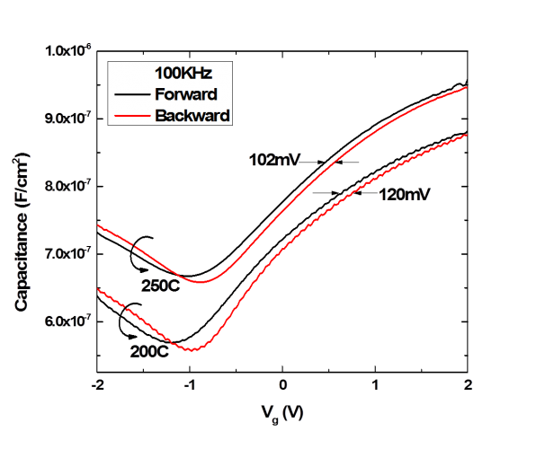
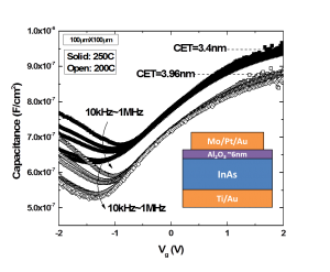
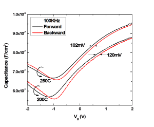
On an S-doped n-type InAs substrate, 60 cycles of Al2O3 are deposited at 200°C and 250°C after HCl wet chemical cleaning. Then, a Mo/Pt/Au (30 nm/20 nm/100 nm) gate stack is formed using electron-beam evaporation; the back contact is formed using Ti/Au. Finally, 30s post-metallization annealing in N2 is carried out. Figure 1 shows the normalized capacitance-voltage (C-V) curves of both samples with frequencies varied from 10kHz to 1MHz. The depletion region of the C-V curve is not sharp and deep, as predicted by simulations [] , which is mainly due to the series capacitance corresponding to Dit. Still, the comparison between the two samples shows that Al2O3 deposited at 200°C yields lower Dit than 250°C. Figure 2 plots the C-V hysteresis of the two samples at 100kHz, which reflects the oxide mobile charge near the interface. The results show that the hysteresis is moderate for both samples and that the ALD dielectric quality is promising. Quantitative analysis of the Dit is ongoing. In summary, InAs/GaSb is a promising heterojunction system, and research is needed to better understand and optimize the dielectric/semiconductor interface.
-
-
Figure 1: C-V curves of InAs MOSCAP with Al2O3 dielectric deposited at 200°C and 250°C. Higher deposition temperature gives slightly higher dielectric constant of the dielectric. Impact of Dit induced series capacitance dominates the depletion behavior of both samples.
-
-
Figure 2: Hysteresis in C-V characteristics of both samples at 100KHz. Mobile charge control in both samples is promising, with hysteresis ~100mV.