A Ballistic Transport Model for HEMTs and III-V MOSFETs
- Category: Materials
- Tags: iii-v materials, jesús del alamo, shireen warnock
As silicon MOSFETs approach the limits of their capabilities, III-V field-effect transistors show promise to replace them. The low-effective mass of various III-V materials such as InGaAs and InAs gives rise to extraordinarily high electron velocities [1] . III-V based High-Electron Mobility Transistors (HEMTs) represent a great model system to understand physics of relevance to future III-V MOSFETs. In HEMTs it is known that as the gate length is reduced to the sub-100-nm regime, the device enters the ballistic regime [2] . In this project, a comprehensive ballistic transport model is being developed to enable the analysis of nanometer-scale III-V HEMTs and MOSFETs and predict the performance of scaled transistors.
The model uses, at its core, a one-dimensional, self-consistent Poisson-Schrödinger simulation of the heterostructure of the transistor. We then add extrinsic device parameters such as source and drain parasitic resistances (RS and RD), as well as appropriate values for the drain-induced barrier lowering (DIBL) and a distribution of interface trap states across the bandgap at the semiconductor surface (Dit). The model uses ballistic transport theory to calculate the current-voltage characteristics of the device. Next, we can display the corresponding transconductance, transfer characteristics, output characteristics, or C-V characteristics. Using an option to graph experimental data on top of simulated data, we can adjust the extrinsic device parameters to fit the simulations to the experiments or to identify discrepancies between the two that indicate where more refined models are needed. In this development phase of the model, we are using HEMTs to calibrate the model’s validity in the various regimes of operation, after which physics of relevance to III-V MOSFETs, such as the effect of Dit and imperfect ballisticity, will be added. Ultimately, our modeling approach will allow us to easily characterize current and future MOSFETs.
-
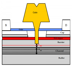
- Figure 1: Schematic of a HEMT structure modeled in this work [3] . The red dotted line in the schematic indicates the location of the δ doping layer, and the channel consists of a composite of InGaAs and InAs. In the simulations shown in Figure 2, a channel of 5-nm InAs was used.

-
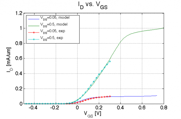
- Figure 2. Experimental versus theoretical transfer characteristics of the HEMT device in Figure 1. Experimental Lg = 30 nm, RS, RD = 240 Ω·μm, DIBL = 80 mV/V, SS = 80 mV/dec. Model RS = 140 Ω·μm, RD = 270 Ω·μm, DIBL = 50 mV/V.
- J. A. del Alamo “Nanometer-scale electronics with III-V compound semiconductors,” Nature, vol. 479, pp. 317-323, Nov. 2011. [↩]
- K. Natori, “Ballistic MOSFET reproduces current-voltage characteristics of an experimental device,” IEEE Electron Device Letters, vol. 23, no. 11, pp. 655-657, Nov. 2002. [↩]
- D. Jin, D.-H. Kim, T.-W. Kim and J. A. del Alamo, “Quantum capacitance in scaled down III-V FETs,” in IEEE Int. Electron Devices Meeting, Baltimore, MD, 2009, pp. 495-498. [↩]