- Authors: H. Zhao, A. Al-Obeidi, C. V. Thompson
- Sponsorship: Iberian Nanotechnology Laboratory-MIT Program,
Silicon nanowires (NWs) have attracted interest for sensing applications due to their high surface-to-volume ratios. When a NW is configured as a field effect transistor (FET), specific binding of chemical and biological species to the NW surface can lead to depletion or accumulation of carriers at the NW surface and result in a significant conductivity change. NW-based biochemical sensing devices for real-time and high sensitivity detection in aqueous solution have been previously reported((Y. Cui, Q. Wei, H. Park, C. M. Lieber, “Nanowire nanosensors for highly sensitive and selective detection of biological and chemical species,” Science, vol. 293, pp. 1289-1292, Aug. 2001.)),[]. However, most NW biochemical sensor studies have focused on devices that have been made using individual nanowires lying on a substrate surface. In contrast, vertical freestanding NW FET sensors have greater potential for very high sensitivity using a minimum of space.
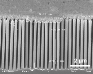
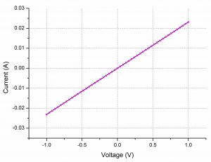
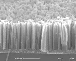
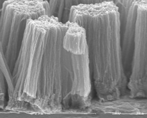
Metal catalyzed etching (MCE) is a low-cost, room-temperature method that enables fabrication of highly ordered Si NW arrays of large aspect ratios with simple processes. Moreover, using various film patterning techniques, we have shown that Si NW arrays can be made in patterned channels[],[] (see Figure 1). Such structures make them very promising for detection of multiple targets in an integrated microfluidic system. A key step in fabricating vertically aligned FET-based sensors is creating a reliable top electrical contact. We have shown that angled evaporation of gold or nickel through a shadow mask can be used to define a top contact (see Figure 2). We have begun work to functionalize and test the sensing performance of the SiNW sensor towards a fully functional, multichannel microfluidic system.
-

-
Figure 1: Vertical silicon nanowire arrays in channels using metal catalyzed etching.
-

-
Figure 2: Au top contact on vertically aligned SiNW arrays using
tilted ebeam evaporation.
- Authors: G. H. Kim, R. V. Zucker, W. C. Carter, W. Bao, D. J. Srolovitz, C. V. Thompson
- Sponsorship: Singapore-MIT Alliance
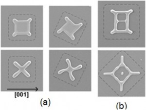
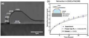
Thin films are generally metastable in the as-deposited state and will dewet (agglomerate) when heated. Nanometer scale films (<100 nm thick) can dewet at temperatures well below the melting temperature of the film, and dewetting occurs while the film remains solid. This phenomenon can limit the use of very thin films in microsystems, but it can also be used to controllably produce complex structures[]. Dewetting occurs through retraction of the edges of naturally forming holes or at patterned edges of films. In single crystal films, anisotropy in surface energy and diffusivity drives the dewetting process to result in regular patterns that relate to the crystal symmetry. We are investigating use of anisotropic dewetting as a self-assembly method to generate complex, small, predetermined patterns. A quantitative understanding of dewetting mechanisms is critical for design of self-assembled structures made through dewetting. We measured the rates of anisotropic edge retraction by solid-state dewetting in kinetically stable edge orientations. These measurements can also be used to estimate the edge retraction rates in a general crystallographic orientation[]. Additionally, an analytical model for solid-state dewetting via surface diffusion for fully faceted materials has been developed to test our understanding of dewetting mechanisms (Figure 1). This two-dimensional model provides excellent agreement with experimental edge retraction rates for kinetically stable edges[]. We also developed a three-dimensional phase-field model for dewetting of materials with isotropic surface energies[]. A three-dimensional model for dewetting of materials with anisotropic surface energies is under development.
-

-
Figure 1: (a) Partially dewetted patches patterned from a (100) film into squares with different in-plane orientations; top is an earlier time than bottom. (b) Dewetting patterns of larger squares[].
-

-
Figure 2: (a) Cross-sectional SEM image of a [010] edge in a (100) film. (b) Corresponding experimental and theoretical retraction distance vs. time[],[].
- Authors: A. Alobeidi, C. V. Thompson.
- Sponsorship: Singapore-MIT Alliance for Research and Technology
Micro-batteries provide a critical component for self-powered autonomous microsystems. Lithium-ion batteries provide relatively high energy storage capacities. Improvement in energy storage capacities over current generation lithium-ion batteries is achievable by using silicon as the anode material. Silicon offers the highest known lithium capacity at the cost of large volume changes, making monolithic silicon structures such as fully dense films or substrates unusable. For silicon-based lithium batteries, nanostructured silicon with high surface-to-volume ratios and superior mechanical properties over bulk are being investigated[],[].
We use metal-catalyzed etching (MCE) to fabricate porous silicon from fully dense silicon films, a process that offers low-cost, room temperature processing of silicon[][][][]. A thin discontinuous metal film is deposited on the silicon and catalyzes the dissolution of silicon when immersed in a solution containing hydrofluoric acid and an oxidant like H2O2. While the monolithic film undergoes significant pulverization and fails in the first few cycles, the porous silicon film shows stable cycling over 25 cycles at a capacity of 2250 mAhg-1 at high rates, expanding nearly three times its size but remaining adherent to the current collector (Figures 1 and 2). Work is currently underway to improve the cyclability of such films and integrate them into solid state batteries for on-chip energy storage.
-

-
Figure 1: Porous amorphous silicon on glass using MCE. This structure is able to accommodate the volume expansion that occurs during lithiation.
-

-
Figure 2: After lithiation, the porous amorphous silicon film breaks into large columnar islands that remain adherent to the current collector.
- Authors: R. Mitchell, B. Gallant, T. Batcho, D. Li, Y. Shao-Horn, C. V. Thompson
- Sponsorship: National Science Foundation, MERSEC
Lithium-air batteries hold promise for the next generation of electric vehicles and other applications. By reacting oxygen directly with lithium ions to form Li2O2 on discharge, these batteries can achieve energy densities 3-5 times higher than current lithium-ion batteries[]. However, a number of challenges exist for implementation, including poor rate capability, poor cyclability, high overpotentials upon charging, and electrode and electrolyte instability[]. We seek to address these issues by developing new electrode materials and architectures.
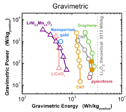
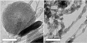
Aligned arrays of carbon nanotubes and nanofibers (CNT/CNFs) provide ideal conducting scaffolds for growth of Li2O2 particles, while the CNT/Fs themselves are low in mass and occupy a small volume fraction of the discharged electrode. We have grown aligned CNFs 5-10 nm in diameter on oxidized silicon substrates and de-laminated them in the form of cohesive carpets. These free-standing conducting carpets were then placed directly into lithium-air cells. We observed near-ideal gravimetric capacities (Figure 1) and high volumetric energy capacities. Control of particle morphology is critical for the high volumetric capacities needed for most applications. Two distinct types of particle morphologies were observed upon discharge, depending on the rate and depth of discharge[]. At low charge rates or high depths of discharge, we observe the formation of large toroid particles. At high rates of discharge, we observe the formation of copious small particles (Figure 2). From x-ray diffraction and selected area electron diffraction, we determined that these are Li2O2 particles with predominantly (0001) surfaces[].
Additionally, we have studied the stability of these carbon nanotube electrodes in a lithium-air cell[]. We observed higher charging overpotentials as the cycle number increased. Using X-ray absorption near edge spectroscopy, we determined that Li2CO3 formed in increasing amounts upon cycling at the interface between lithium peroxide and the carbon nanotube [4]. We attribute poor cycling performance and higher charge overpotentials to this Li2CO3 formation, possibly due to reaction of Li2O2 with the CNTs. We are currently carrying out research to address this issue.
-

-
Figure 1: A plot of the gravimetric power and energy of CNT and CNF batteries as compared to other lithium-air and lithium-ion cathodes and the theoretical limit of gravimetric energy[].
-

-
Figure 2: Lithium peroxide particles formed at (a) low charge rates or high depth of discharge, and (b) at high charge rates.
