Silicon Nanowires for Chemical Sensing Systems
- Category: Nanotechnology
- Tags: carl thompson, kathleen fitzgerald
Silicon nanowires (NWs) have attracted interest for sensing applications due to their high surface-to-volume ratios. When a NW is configured as a field effect transistor (FET), specific binding of chemical and biological species to the NW surface can lead to depletion or accumulation of carriers at the NW surface and result in a significant conductivity change. NW-based biochemical sensing devices for real-time and high sensitivity detection in aqueous solution have been previously reported((Y. Cui, Q. Wei, H. Park, C. M. Lieber, “Nanowire nanosensors for highly sensitive and selective detection of biological and chemical species,” Science, vol. 293, pp. 1289-1292, Aug. 2001.)),[1]. However, most NW biochemical sensor studies have focused on devices that have been made using individual nanowires lying on a substrate surface. In contrast, vertical freestanding NW FET sensors have greater potential for very high sensitivity using a minimum of space.
Metal catalyzed etching (MCE) is a low-cost, room-temperature method that enables fabrication of highly ordered Si NW arrays of large aspect ratios with simple processes. Moreover, using various film patterning techniques, we have shown that Si NW arrays can be made in patterned channels[2],[3] (see Figure 1). Such structures make them very promising for detection of multiple targets in an integrated microfluidic system. A key step in fabricating vertically aligned FET-based sensors is creating a reliable top electrical contact. We have shown that angled evaporation of gold or nickel through a shadow mask can be used to define a top contact (see Figure 2). We have begun work to functionalize and test the sensing performance of the SiNW sensor towards a fully functional, multichannel microfluidic system.
-
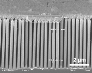
- Figure 1: Vertical silicon nanowire arrays in channels using metal catalyzed etching.
-
- Figure 2: Au top contact on vertically aligned SiNW arrays using tilted ebeam evaporation.
- E. Stern, J. F. Klemic, D. A. Routenberg, P. N. Wyrembak, D. B. Turner-Evans, A. D. Hamilton, D. A. LaVan, T. M. Fahmy, M. A. Reed, “Label-free immunodetection with CMOS-compatible semiconducting nanowires,” Nature, vol. 445, pp. 519-522, Feb. 2007. [↩]
- S. W. Chang, V. P. Chuang, S. T. Boles, C. A. Ross, and C. V. Thompson, “Densely packed arrays of ultra‐high‐aspect‐ratio silicon nanowires fabricated using block‐copolymer lithography and metal‐assisted etching,” Advanced Functional Materials, vol. 19, pp. 2495-2500, Aug. 2009 [↩]
- S. W. Chang, V. P. Chuang, S. T. Boles, and C. V. Thompson, “Metal‐Catalyzed etching of vertically aligned poly-silicon and amorphous Silicon Nanowire Arrays by Etching Direction Confinement,” Advanced Functional Materials, vol. 20, pp. 4364-4370, Dec. 2010. [↩]