- Authors: E. Timurdogan, E. S. Hosseini, G. Leake, D. D. Coolbaugh, M. R. Watts
- Sponsorship: DARPA
Silicon photonics enables wavelength-division multiplexed (WDM) networks to be efficiently and cost effectively implemented on chip with potential for multi-terabit/s communication links. Microring-based filters perform the multiplexing and demultiplexing operations and require tight alignment between the laser line and filter resonances, which drift by process/wafer variations and dynamic temperature fluctuations. Therefore, high-speed thermo-optic control of microring filters is necessary in silicon photonic communication links. The challenge is in implementing such control efficiently. Without using complex undercut etch processes, the most efficient thermo-optic tunable filters to date have been demonstrated with a 4.4 µW/GHz tuning efficiency, 1-µs thermal time constant, and a free spectral range (FSR) of 5.6 THz[]. For a WDM link with ± 200C variation due to processor activity, thermal tuning will consume ~1.8 mW ((M. R. Watts , W. A. Zortman , D. C. Trotter , G. N. Nielson , D. L. Luck and R. W. Yong “Adiabatic resonant microrings (ARMs) with directly integrated thermal microphotonics”, in Proc. Conf. Lasers Electro-Opt., pp.1 -2 2009.)) power as opposed to an integrated microdisk modulator with a 3-fJ/bit performance and a power consumption of 30 µW at a data rate of 10 Gb/s[]. Therefore, it is essential to introduce new resonators. Additionally, high-speed thermal tuning can enable reconfigurable networks as well as track the dynamic processor activity. However, the buried oxide thickness around the microring filter favors either thermal tuning efficiency or speed.
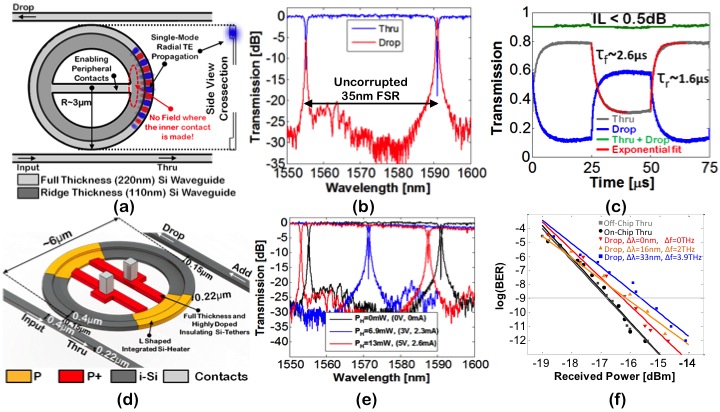
In this paper[], we introduce a new class of filters, L-shaped resonant microrings (LRM) (Figure 1), which allow for both hard outer walls and single mode propagation (Figure 1a-b) while enabling interior electrical contacts without inducing radiation or scattering. Thus, LRM filters (Figure 1d) can directly integrate a heater within the resonator, minimize the thermal capacitance, and maintain a compact size and an uncorrupted FSR (Figure 1b). Here, we demonstrate a 6-um diameter LRM filter (Figure 1d) with high efficiency (3.3 µW/GHz), high-speed (1.6 µs) thermal tuning (Figure 1c,e) and record low through-to-drop power penalty (<1.1 dB) (Figure 1f) over the 4 THz FSR (Figure 1b).

Figure 1: a) Finite difference time domain (FDTD) simulation of an LRM resonator. b) Measured spectrum of the fabricated LRM filter, showing uncorrupted 4-THz FSR on through and drop ports. c) Temporal response of the thru and drop ports of the LRM filter, excited by 20kHz 0.15V square-wave drive, fit to a 2.6-µs exponential decay and a 1.6-µs rise thermal time constant (shown in red), the insertion loss (IL) of the LRM filter is
- Authors: E. Timurdogan, C. M. Sorace-Agaskar, M. R. Watts
- Sponsorship: DARPA, NSF-GRFP
On- and off-chip bandwidth and energy scaling are pushing the limits of CMOS and VCSEL technology, which allow only a single channel per fiber or wire. Wavelength-division multiplexed (WDM) systems based on silicon photonic interconnects can enable high-bandwidth, energy-efficient communications. Integrated resonant modulators play a major role in such links. Resonant silicon modulators utilize the plasma dispersion effect through free-carrier injection or depletion of a diode. Compact 3.5-μm microdisk modulators have been demonstrated with a power consumption of only 3 fJ/bit at 1-Vpp and 12.5 Gb/s operation[]. Recently, 25Gb/s operation with 13fJ/bit at 1.2Vpp has been demonstrated with ~6-μm diameter microdisk modulator[]. However, the microdisk inherently supports spurious modes that corrupt the free spectral range (FSR) by introducing unwanted resonance dips on the transmission. Therefore, only half of the FSR can be used for WDM channels in a silicon photonic link. Microrings eliminate the undesired modes, but directly contacting the microring induces scattering loss. External ridge based modulators increase the diameter to ~5-10 μm due to low confinement, thereby increasing the area and power. Recently, a 4-μm diameter adiabatic resonant microring modulator, which enabled single-mode operation by adiabatic tapering of the single mode waveguide, was demonstrated but limited to 12.5 Gb/s operation due to electrical resistance of the contacts[].
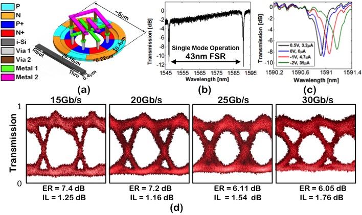
In our paper[], we introduce a new class of modulators, L-shaped resonant microrings (LRM) (Figure 1a), which allow for both hard outer walls and single mode propagation while maintaining low resistance electrical contacts. Thus, LRM modulators can have a compact size, high quality factor, and an uncorrupted FSR (Figure 1b) while maintaining high-speed operation. To allow for interior contacts, a hybrid junction consisting of a vertical and interdigitated p-n junction (Figure 1a) is formed. Frequency shifts and spectral response are shown in Figure 1c. Here, we demonstrate the LRM modulator operating in depletion mode, with data rates up to 30 Gb/s (Figure 1d), occupying chip area of < 20 µm2 and maintaining an uncorrupted 5.3 THz FSR (Figure 1b).

Figure 1: a) 3D sketch of the LRM modulator showing size, doping, and metal connections. b) Spur-free single mode operation of the LRM modulator with an FSR of 5.3 THz. c) Spectral response of the LRM modulator with respect to voltage dropped and current passing through the device. d) High speed measured optical eye diagrams at 15-, 20-, 25-, and 30-Gb/s data rates of the LRM modulator, driven by a PRBS data of 2.2Vpp with a -0.6V DC bias. Dynamic insertion loss and extinction ratio are denoted below the eye diagrams.
- Authors: E. Timurdogan, C. M. Sorace-Agaskar, G. Leake, D. D. Coolbaugh, M. R. Watts
- Sponsorship: DARPA, NSF-GRFP
Wavelength division multiplexed systems can achieve high bandwidth by utilizing many channels on a single fiber as opposed to current single channel per cable or fiber interconnects. Silicon photonics can readily enable wavelength-division multiplexed (WDM) systems through the use of compact, inherently wavelength selective micro-ring/-disk resonators. Such devices have been demonstrated to have energies as low as 3fJ/bit at a data rate of 12.5Gb/s[] and 13fJ/bit at a data rate of 25Gb/s[]. However, resonance drifts, induced by process/wafer variations and dynamic temperature fluctuations, detune the alignment between the modulators and the WDM lasers and need to be compensated. Electro-optic tuning can compensate only for temperature variations of ~± 2.50C, while processor core activity on chip yields temperature fluctuations on the order of ±100C. Therefore, thermo-optic tuning and control of resonators is required[].
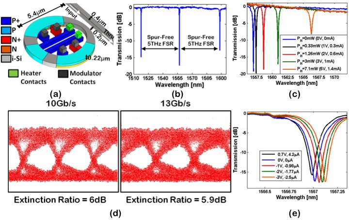
Here[], we demonstrate a 5.4-µm-diameter adiabatic resonant microring (ARM) modulator with a CMOS compatible integrated heater (Figure 1a) allowing for single mode operation (Figure 1b), high performance modulation and minimum thermal capacitance. High-speed modulation (Figure 1d) is achieved through a vertical p-n junction around the edge of the ARM modulator and low resistance interior contacts. Electro-optic frequency shifts and spectral response are shown in Figure 1e. The proposed ARM modulator is measured to have a 6.2µW/GHz thermal tuning efficiency (Figure 1c), ~9fJ/bit modulation performance at a data rate of 13Gb/s (Figure 1d), and a 5.9dB extinction ratio. This is the first demonstration of an integrated heater and modulator within an ARM resonator and the most compact microring modulator with a directly integrated heater.

Figure 1: a) 3D sketch of the ARM modulator with integrated heater showing size, doping and contacts. b) Spur-free single mode operation of the LRM modulator with a FSR of 5 THz. c) Measured DC spectral response of the integrated heater inside the ARM modulator with an applied bias voltage to heater pins. d) High-speed optical eye diagrams at a data rate of 10- and 13-Gb/s with a 1.8Vpp (0 to -1.8V) drive. The extinction ratio is 6dB. e) Measured spectral response of the ARM modulator with applied DC bias voltage to modulator pins from -3V to 0.7V.
- Authors: E. Timurdogan, C. M. Sorace-Agaskar, E. S. Hosseini, G. Leake, D. D. Coolbaugh, M. R. Watts
- Sponsorship: DARPA, NSF-GRFP
Silicon photonics, because it enables wavelength division multiplexed (WDM) systems, will help to minimize the number of fibers required in high performance computing (HPC) machines. It also promises to do so with low power and high-speed resonant devices. Resonant electro-optic modulators will likely be used to transmit data in the WDM links and have been demonstrated to have energies as low as 3fJ/bit at a data rate of 12.5Gb/s[] and 13fJ/bit at a data rate of 25Gb/s[]. However, resonance drifts, induced by process/wafer variations and dynamic temperature fluctuations, distort the alignment between the modulators and the desired WDM channels. Electro-optic tuning can be used for temperature variations of ~± 2.50C. However, processor core activity on chip yields temperature fluctuations on the order of ±100C. Therefore, thermo-optic control of the resonators is necessary[]. The integration of heaters within microring filters and modulators achieves the best optimization of thermal tuning power (4.4 µW/GHz) and speed (1 µs)[].
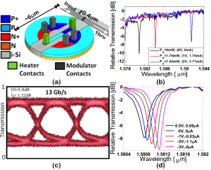
In our work[], we propose a ~6-µm diameter (footprint ~ 28 µm2) microdisk modulator with a CMOS compatible integrated heater in the center that allows for high performance modulation and minimum thermal capacitance (Figure 1a). The hard outer walls of the microdisk modulator enable minimum bend radii and high-Q operation (Figure 1a-b). A vertical p-n junction near to the edge of the microdisk modulator and low resistance interior contacts enables high-speed modulation (Figure 1c). Frequency shifts and spectral response are shown in Figure 1d. The proposed microdisk modulator is measured to have a 4.9µW/GHz thermal tuning efficiency (Figure 1b) and ~11fJ/bit performance at a data rate of 13 Gb/s (Figure 1c), a 5.8dB extinction ratio, and a 1.22dB insertion loss. This is the most efficient heater integration into a modulator; the first modulator exhibits total modulation and heater energy <50fJ/bit for a realistic modulator performance.

Figure 1: a) 3D sketch of the microdisk modulator with integrated heater showing size, doping and contacts. b) Measured DC spectral response of the integrated heater inside the microdisk modulator with an applied bias voltage to heater pins. c) High-speed optical eye diagrams at a data rate of 13-Gb/s with an ac-coupled 1.5Vpp drive and 2V applied across heater contacts. The extinction ratio is 5.8dB and insertion loss is 1.22dB. d) Measured spectral response of the microdisk modulator with applied DC bias voltage to modulator pins from -3V to 0.5V.
- Authors: E. Timurdogan, C. M. Sorace-Agaskar, A. Biberman, M. R. Watts
- Sponsorship: DARPA, NSF GRFP
High-performance computing systems require high bandwidth, low power, and scalable optical interconnects to maintain balanced communications in future exascale machines. Low-power, low-voltage, high-speed, and compact CMOS-compatible silicon electro-optic modulators are key enablers for next generation optical interconnects. Silicon modulators based on the free-carrier effect in silicon achieve high-speed modulation by injecting or depleting charge, inducing a frequency shift in a Mach-Zehnder interferometer or resonant device that translates the resultant frequency shift into an amplitude response. Resonant modulators confine light in compact high-Q devices, enhancing the interaction of the light with the change in charge distribution. Compact resonant devices also minimize the device capacitance, enabling high-speed and low power modulators. In previous record-setting demonstrations, vertical p-n junction devices have achieved error-free modulation up to 12.5Gb/s with only a 1V drive and while consuming only 3fJ/bit[].
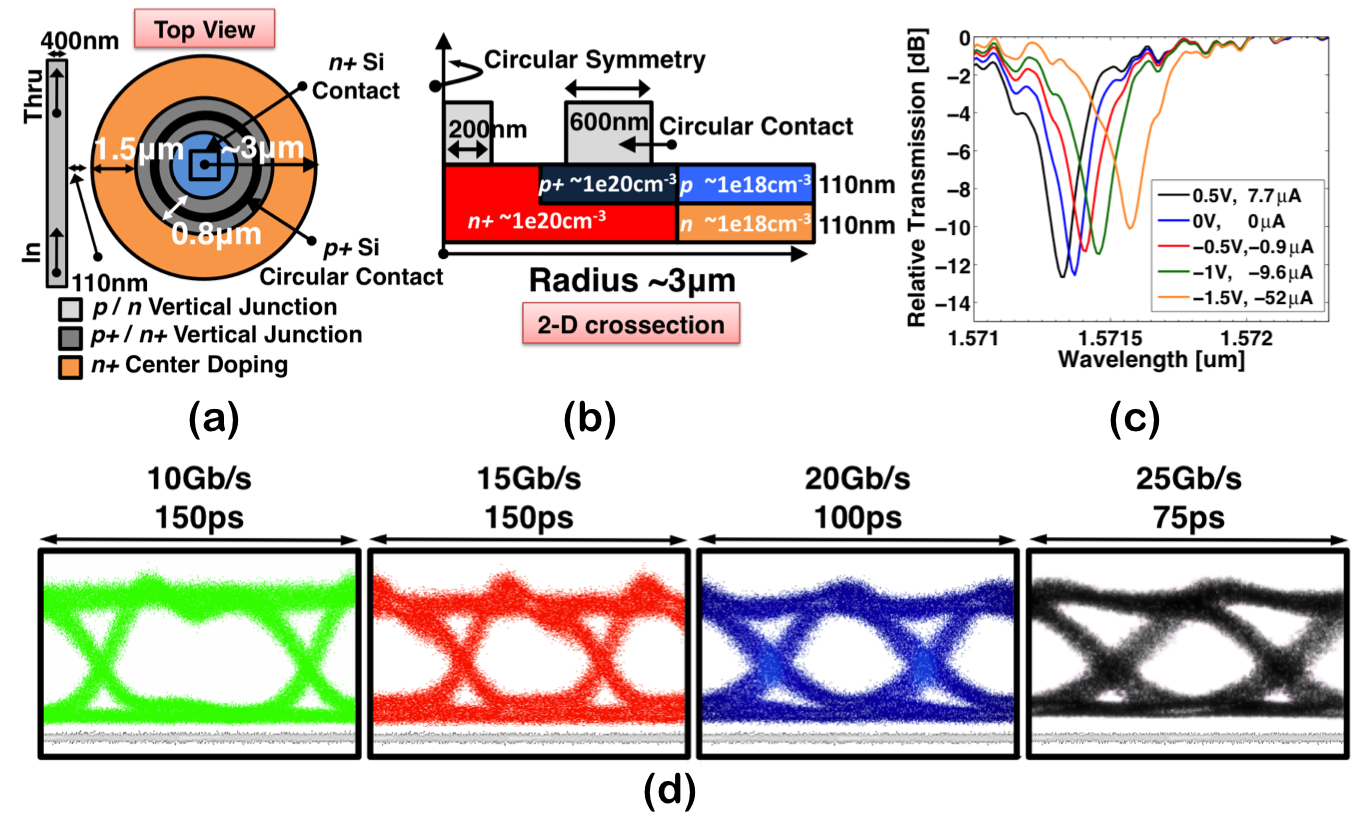
In our work[], we experimentally demonstrate the first vertical junction silicon microdisk modulator (Figure 1a-b) to achieve open eye-diagrams at a data rate of 25Gb/s (Figure 1d) and error-free operation up to 20Gb/s. A circular overlapping p+ and n+ doping profile within circularly contacted microdisk modulators (Figure 1a-b) reduce the device resistance and enable high-speed operation while maintaining a hard outer wall for maximizing the optical confinement. Frequency shifts and spectral response is shown in Figure 1c. The device represents the smallest silicon modulator to run at 25Gb/s and achieves the lowest reported power penalty compared to a commercial LiNbO3 modulator [2], important for the overall power budget in a microphotonic link.

Figure 1: a) Top-view of the 6-µm-diameter microdisk modulator, which utilizes circular inner contacts. b) 2D cross-section showing the doping profile with p-n vertical junction, p+and n+ overlapping regions. c) Spectral response of the microdisk modulator with respect to voltage dropped and current passing through the microdisk modulator. d) High-speed measured optical eye diagrams at 10-, 15-, 20-, and 25-Gb/s data rates of the microdisk modulator, driven by AC coupled 1.2Vpp. The eye diagrams are shown with the true zero (gray line) at each data rate.
